Method for preparing GaN-based pattern substrate template

A graphic substrate and template technology, applied in semiconductor/solid-state device manufacturing, electrical components, circuits, etc., can solve the problems of complex process, expensive equipment, high cost, etc., and achieve the effect of simple preparation, low cost and fast speed

Inactive Publication Date: 2010-08-25
SUN YAT SEN UNIV
View PDF2 Cites 14 Cited by
  • Summary
  • Abstract
  • Description
  • Claims
  • Application Information

AI Technical Summary

Problems solved by technology

Substrates with smaller pattern sizes are usually prepared by electron beam lithography or X-ray lithography, but these advanced lithography equipment is expensive and the process is complicated, not only the cost is high, but the yield is also low

Method used


Image

  • Method for preparing GaN-based pattern substrate template
  • Method for preparing GaN-based pattern substrate template
  • Method for preparing GaN-based pattern substrate template

Examples


Embodiment Construction

[0031] The present invention will be described in detail below in conjunction with the accompanying drawings.

[0032] As shown in FIGS. 1 to 5 , this embodiment is described by taking the preparation method of a submicron-scale patterned GaN substrate on a sapphire substrate as an example.

[0033] The preparation method of the GaN-based graphic substrate template of the present embodiment comprises the following steps:

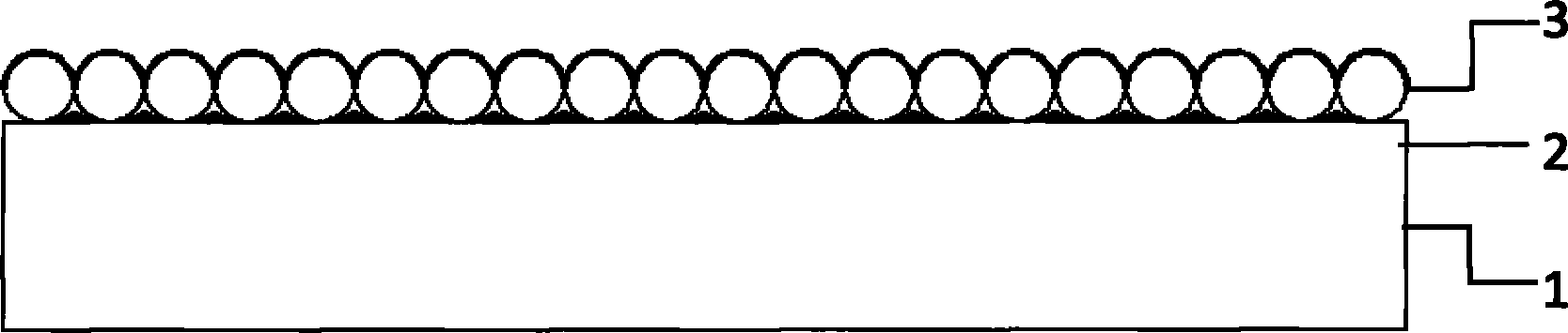
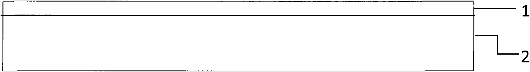
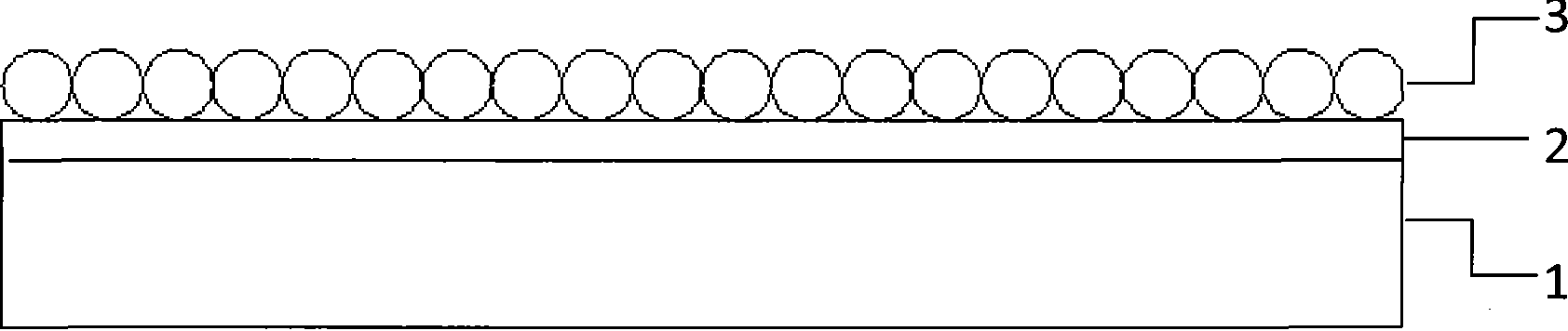
[0034] Step 1: A GaN film with a thickness of 2 microns is grown on a sapphire substrate 1 by MOCVD as a GaN template 2 for nitride growth, as shown in FIG. 1 .

[0035] Step 2: Then, mix the polystyrene microspheres with ethanol to prepare a mixed solution, and spin-coat the mixed solution on the surface of the GaN template 2, and the polystyrene microspheres will gather into a monolayer structure to form a microsphere layer 3 such as figure 2.

[0036] Step 3: Next, deposit 10nm metallic gold on the surface of the sample by means of electron beam evapora...


PUM

PropertyMeasurementUnit
thicknessaaaaaaaaaa

Abstract

The invention relates to a method for preparing a GaN-based pattern substrate template. The method comprises the following steps of: growing a layer of GaN-based template on a substrate for epitaxial growth of nitrides; laying microspheres on the surface of the GaN-based template by using a microsphere solution to form a microsphere layer with a monomolecular layer structure; evaporating metals on the substrate, depositing the evaporated metals on the surface of the GaN-based template through the voids among the microspheres; removing the microsphere layer with a monomolecular layer structure by supersonic vibration to obtain a pattern metal layer; transferring patterns on the metal layer to the GaN-based template with an etching method by using the metal layer as a mask; and removing the metal layer to obtain the GaN-based material pattern substrate template. The method has the advantages of simple process, low cost and adjustable pattern pit size and space. The method can be used for preparing a micron-grade semiconductor substrate pattern.

Description

technical field [0001] The invention relates to the field of semiconductor material growth, in particular to a preparation method of a GaN-based pattern substrate template. Background technique [0002] Nitride compound semiconductor materials represented by III-V gallium nitride (GaN) materials are widely used in violet light-emitting diodes, violet lasers, ultraviolet light detectors, and high-power high-frequency electronic devices. Due to the lack of suitable substrate materials, the current epitaxy of high-quality GaN-based materials is grown on heterogeneous substrates such as sapphire, SiC, and Si. However, there is a large lattice mismatch and thermal expansion coefficient mismatch between the heterogeneous substrate and GaN-based materials. This will result in a large stress and crystal defect density in GaN-based material epitaxial layers grown by epitaxial techniques such as metal organic chemical vapor deposition (MOCVD), hydride vapor phase epitaxy (HVPE) or mo...

Claims


Application Information

Patent Timeline
Patent Type & Authority Applications(China)
IPC IPC(8): H01L21/033
Inventor 张佰君卫静婷饶文涛
Owner SUN YAT SEN UNIV
Why Eureka
Try Eureka