Minitype capacitance type gas sensor and preparation method thereof
A technology of gas sensor and microcapacitance, which is applied in fluid pressure measurement, ion implantation plating, coating and other directions using capacitance changes, and can solve the problems of small adsorption area, unfavorable gas contact, long response time, etc.
- Summary
- Abstract
- Description
- Claims
- Application Information
AI Technical Summary
Problems solved by technology
Method used
Image
Examples
preparation example Construction
[0038] The preparation method includes the following steps:
[0039] ①Prepare the bottom electrode film on the silicon substrate and pattern it to form the bottom electrode plate;
[0040] ②Silicon nitride or silicon oxynitride film is prepared on the bottom electrode plate by chemical vapor deposition method, and the film is etched to form pillars. The shape of the pillars at the peripheral edges may be inconsistent with the pillars at the center, and the size may also be larger than that at the center;
[0041] ③The thickness of spin-coated glass is consistent with the height of the pillar;
[0042] ④Prepare doped polysilicon on the sacrificial glass layer by chemical vapor deposition as the upper electrode plate to form a plate capacitor;
[0043] ⑤Use HF acid to remove the sacrificial glass layer, release the cavity structure, and form a flat capacitor with a cavity structure;
[0044] ⑥The dipping method is adopted to coat the dielectric film on the support of the flat capacitor wit...
Embodiment 1
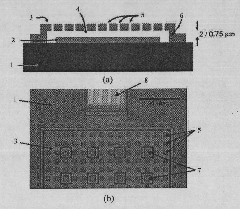
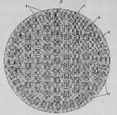
[0049] Such as image 3 As shown, the shape of the sensor is circular and the pillar is square. The gas sensor of this structure includes a lower electrode plate 2, an upper electrode plate 3, a pillar 7, a dielectric sensitive film 4, an air hole 5 arranged on the side wall, and a side wall 6 with openings. A metal aluminum film with a thickness of 500 nm is deposited on the silicon substrate 1 through an evaporation process, and the film is patterned by photolithography to form a circle with a diameter of 1 mm as the bottom electrode plate 2 of the flat capacitor. The sidewalls 6 and pillars 7 are made of silicon nitride, and the film thickness is 2um. They are prepared by a plasma enhanced chemical vapor deposition (PECVD) process and formed by dry etching image 3 The pattern shown. The side walls 6 are fan-shaped pillars separated from each other with a duty ratio of 1:1. The center angles of the fan-shaped pillars and the air holes 5 are both 4.5°; the inner pillar 7 is a...
Embodiment 2
[0051] The shape of the sensor in this example is round, and the pillar is also round, such as Figure 4 Shown. Compared with Example 1, the lower electrode plate 2, the side walls 6, the dielectric sensitive film 4 and the upper electrode plate 3 of the sensor are the same, except that the dielectric layer pillar 7 is designed to be circular. The circular pillars 7 have a height of 2um, a diameter of 50um, and have a horizontal interval of 150um and a vertical interval of 50um, and they are staggered on the bottom electrode plate 2.
PUM
| Property | Measurement | Unit |
|---|---|---|
| Diameter | aaaaa | aaaaa |
Abstract
Description
Claims
Application Information


