Trench type semiconductor power device with low gate resistance and preparation method thereof

A technology for power devices and semiconductors, applied in the field of new and improved cell structure and device configuration, can solve the problems of difficult process, increase gate resistance, limit cell density, etc., achieve simple production, reduce internal gate resistance, and improve cell density. Effect

Active Publication Date: 2010-09-08
M-MOS半导体香港有限公司
View PDF3 Cites 6 Cited by
  • Summary
  • Abstract
  • Description
  • Claims
  • Application Information

AI Technical Summary

Problems solved by technology

[0004] Disadvantages: When the trench width becomes smaller, the doped polysilicon in the trench area decreases, and the gate resistance increases, especially for the trench in the central area, which affects the switching speed of the device
[0006] Disadvantages: The source metal is divided into several pieces, which will increase the Ron value of the

Method used


Image

  • Trench type semiconductor power device with low gate resistance and preparation method thereof
  • Trench type semiconductor power device with low gate resistance and preparation method thereof
  • Trench type semiconductor power device with low gate resistance and preparation method thereof

Examples


Embodiment Construction

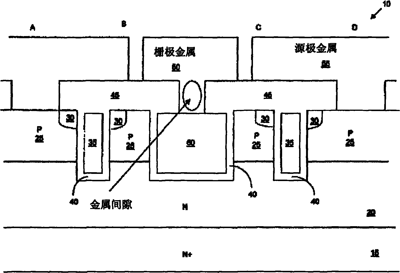
[0048] The trench type semiconductor power device with low gate resistance of the present invention, in order to reduce the gate resistance, a buried trench type gate 250 with titanium / titanium nitride / tungsten plugs is formed, with an NSG layer 270 on the top, The buried trench gate 250 arrangement is one standard trench gate with one buried trench gate, or 10 standard trench gates with one buried trench gate ; The number of the buried trench gate 250 is inversely proportional to the width of the standard trench gate of the unit, and is inversely proportional to the required gate resistance value. With the new invention, the gate resistance is not limited by the small cell pitch.

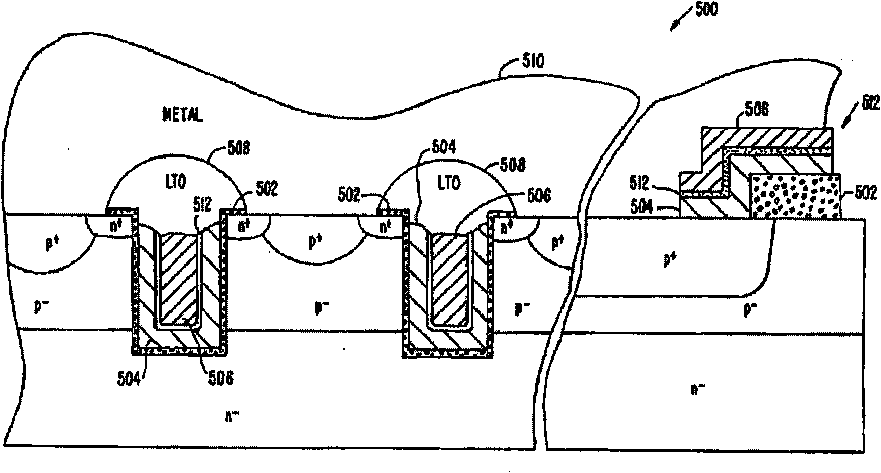
[0049] The following figure ( Figure 5A to Figure 5H ) in the X-direction sectional view of the technological process for demonstrating the idea of ​​the present invention: in Figure 5A In , a trench mask is used to form trenches 208 in epitaxial layer 210 on base layer 205 .

[0050] exist ...


PUM


Abstract

The invention relates to a trench type semiconductor power device with low gate resistance and a preparation method thereof, the semiconductor power device comprises an embedded trench type gate (250) with a titanium/titanium nitride/tungsten plug, an NSG layer (270) is arranged at the top, the arrangement of the embedded trench type gate (250) is that a standard trench gate is matched with the embedded trench type gate, or 10 standard trench gates are matched with the embedded trench type gate; and the number of the embedded trench type gate (250) is inversely proportional to the width of the unit standard trench gate and inversely proportional to the required gate resistance. The device and the preparation method thereof can reduce the internal gate resistance, simultaneously not affectthe improvement of the unit density, simplify the manufacture and be applicable to mass production. The trench type semiconductor power device can be used for a variety of trench type metal oxide semiconductor field effect transistors, such as P type and N type low-voltage devices and high-voltage devices, P type and N type IGBT, high-voltage integrated circuits and the like.

Description

technical field [0001] The present invention relates to a cell structure and device configuration of a power semiconductor device. More particularly, the present invention relates to a new and improved cell structure and device configuration for trench-type semiconductor power devices with low gate resistance. Background technique [0002] Conventional techniques for forming trenched gates and gates for high-density trenched metal-oxide-semiconductor field-effect transistor (Mosfet) devices are facing technical difficulties, as the undesirable internal gate resistance increases as the trench width decreases As a result, the switching speed becomes slower. Narrow trench widths result in high gate resistance due to reduced doped polysilicon in the trench region. High gate resistance can adversely affect the switching performance of the device and also reduce product reliability. [0003] refer to Figure 1A and 1B , a top view and a side cross-sectional view of a common Mo...

Claims


Application Information

Patent Timeline
IPC IPC(8): H01L29/41H01L29/78H01L21/336H01L21/283
Inventor 苏冠创
Owner M-MOS半导体香港有限公司
Why Eureka
Try Eureka