Manufacturing process for realizing through silicon via packaging by adopting BCB (Benzocyclobutene) supplementary bonding

A manufacturing process and through-silicon via technology, which is applied in semiconductor/solid-state device manufacturing, electrical components, circuits, etc., can solve the problems of low bonding strength, high metal bonding strength, and high cost of sputtering metal, and achieve a reduction in process Cost, improved yield, and simple process

Inactive Publication Date: 2010-09-15
SHANGHAI INST OF MICROSYSTEM & INFORMATION TECH CHINESE ACAD OF SCI
View PDF2 Cites 21 Cited by
  • Summary
  • Abstract
  • Description
  • Claims
  • Application Information

AI Technical Summary

Problems solved by technology

Metal bonding is to bond two wafers with metal surfaces sputtered with each other. This method has high metal bonding strength and can also be used as a seed layer for electroplating TSV. However, the cost of sputtering metal is high and the bonding temperature very high
The photoresist bonding process is simple, but the bonding strength is low, and the wafers are easy to fall off in the subsequent process, and due to the fluidity of the resist during bonding, it is easy to cause uneven thickness of the bonding interface, which affects the subsequent process. Negative Effects

Method used


Image

  • Manufacturing process for realizing through silicon via packaging by adopting BCB (Benzocyclobutene) supplementary bonding
  • Manufacturing process for realizing through silicon via packaging by adopting BCB (Benzocyclobutene) supplementary bonding
  • Manufacturing process for realizing through silicon via packaging by adopting BCB (Benzocyclobutene) supplementary bonding

Examples


Embodiment Construction

[0014] In order to fully demonstrate the advantages and positive effects of the present invention, the present invention will be further described below in conjunction with the accompanying drawings and embodiments.

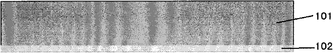
[0015] exist figure 1 In this method, a layer of Au layer 102 with strong oxidation resistance is sputtered on one side of the bare support wafer 101 with a thickness of about 100-200 nm. The role of this metal layer is to provide a seed layer for TSV electroplating Cu.

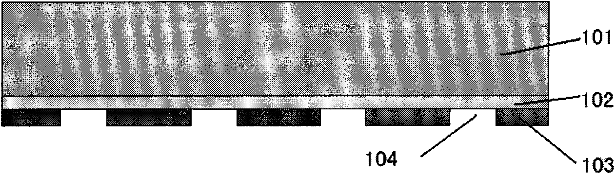
[0016] exist figure 2 In this method, a layer of BCB103 is coated on the metal layer 102 of the bare support wafer 101, and the thickness of the BCB is about 2-4 μm. The BCB is shaped by photolithography, so that the BCB at the position 104 to be bonded to the TSV through hole is removed.

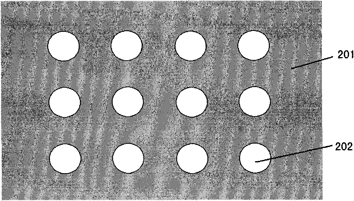
[0017] exist image 3 in SiO 2 As a mask, DRIE is used to etch the front side of the TSV wafer 201 to form a TSV array pattern 202, but the TSV wafer is not completely etched through, leaving a certain ...


PUM

PropertyMeasurementUnit
thicknessaaaaaaaaaa
thicknessaaaaaaaaaa

Abstract

The invention relates to a manufacturing process for realizing through silicon via packaging by adopting BCB (Benzocyclobutene) supplementary bonding. The manufacturing process is characterized being a method for manufacturing the TSV (Through Silicon Via) packaging after a wafer is thinned under the assistance of a support wafer which is bonded at low temperature by utilizing organic matter BCB. The manufacturing process of the TSV packaging comprises the following steps of: sputtering a metal layer on the naked support wafer, coating a layer of BCB and then carrying out photoetching; carrying out DRIE (Deep Reactive Ion Etching) on the front face of the TSV wafer to form a TSV array; aligning one side of the support wafer with the BCB with the front face of the TSV wafer and then carrying out BCB low-temperature bonding in a bonding machine; and manufacturing TSV subsequent process after the TSV wafer is thinned. The TSV packaging manufacturing process has higher reliability, and the adopted device and the adopted process are both a conventional process and a device in the semiconductor machining.

Description

technical field [0001] The present invention relates to a manufacturing process of using BCB assisted bonding to realize through-silicon via (Through silicon via TSV) packaging. The method for making TSV after thinning belongs to the technical field of wafer-level TSV three-dimensional interconnection packaging. Background technique [0002] In order to meet the needs of the development of very large scale integration (VLSI), a novel 3D stacked packaging technology emerged as the times require. It integrates chips of different performance and multiple technologies into a single package with the smallest size and lightest weight. It is a kind of vertical electrical conduction between chips and wafers. , the packaging and interconnection technology that realizes the interconnection between chips, and the difference from the previous IC package bonding and bump technology is that the described process uses TSV (Through Silicon Via, Through Silicon Via) instead of 2D- Cu inter...

Claims


Application Information

Patent Timeline
Patent Type & Authority Applications(China)
IPC IPC(8): H01L21/768
Inventor 陈骁罗乐徐高卫袁媛
Owner SHANGHAI INST OF MICROSYSTEM & INFORMATION TECH CHINESE ACAD OF SCI
Why Eureka
Try Eureka