GaN-based flip-chip light-emitting diode with double reflecting layers and preparation method thereof

A light-emitting diode, gallium nitride-based technology, applied in electrical components, circuits, semiconductor devices, etc., can solve the problems of reduced reflectivity of metal reflective layers, low surface resistance, and high production costs of high-brightness LEDs, and achieves improved luminous efficiency, The effect of excellent reflectivity

Inactive Publication Date: 2010-10-13
XIAMEN SANAN OPTOELECTRONICS TECH CO LTD
View PDF5 Cites 58 Cited by
  • Summary
  • Abstract
  • Description
  • Claims
  • Application Information

AI Technical Summary

Problems solved by technology

[0002] Light-emitting diodes have the advantages of small size, high brightness, low power consumption, and long life. With the continuous improvement of the light efficiency of power-type GaN-based LEDs, it is the general trend for LED lamps to replace traditional lighting sources. However, the production cost of high-brightness LEDs is high. Low efficiency, so high-brightness LEDs are still difficult to promote and apply on a large scale
[0003] Chinese invention patent (publication number CN1622349A) discloses a flip-chip light-emitting diode and its manufacturing method. , fluorine, phosphorus, arsenic at least one ohmi

Method used


Image

  • GaN-based flip-chip light-emitting diode with double reflecting layers and preparation method thereof
  • GaN-based flip-chip light-emitting diode with double reflecting layers and preparation method thereof
  • GaN-based flip-chip light-emitting diode with double reflecting layers and preparation method thereof

Examples


Embodiment Construction

[0031] The present invention will be further described below in conjunction with the accompanying drawings and embodiments.

[0032] The preparation process of gallium nitride-based flip-chip light-emitting diodes with a double reflection layer of a distributed Bragg reflection layer and a metal reflection layer, the steps are as follows:

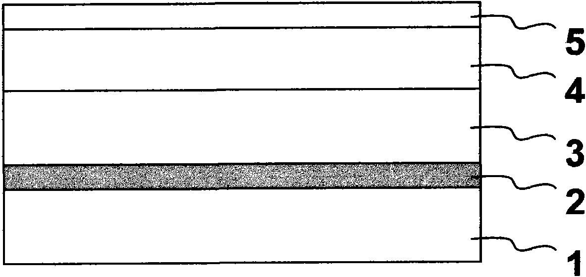
[0033] Such as figure 1 As shown, a GaN buffer layer 2, an N-GaN layer 3, a multi-quantum well layer 4 and a P-GaN layer 5 are sequentially grown on a sapphire substrate 1;

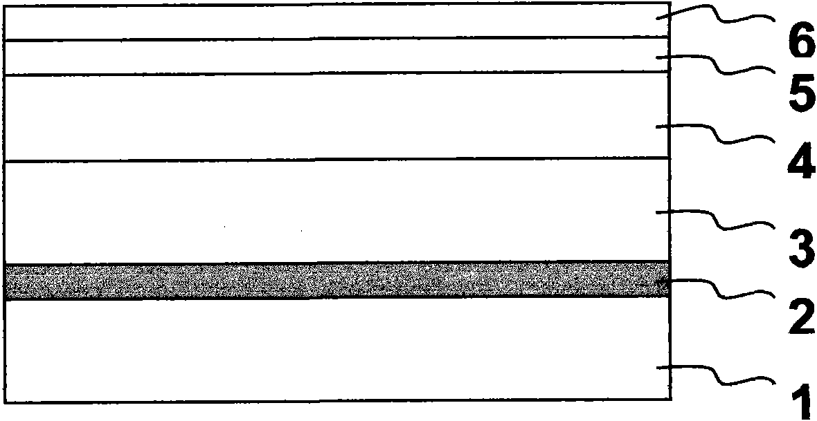
[0034] Such as figure 2 As shown, an ITO transparent conductive layer 6 is formed on the P-GaN layer 5;

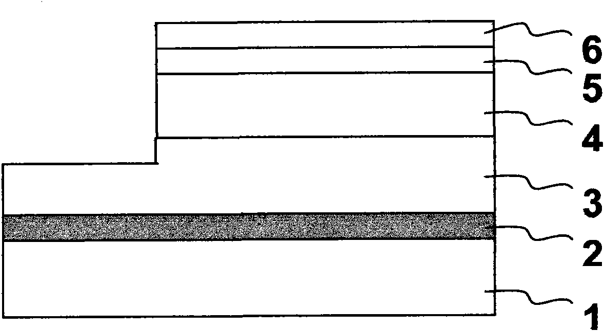
[0035] Such as image 3 As shown, through a photomask and etching, the part of the mesa where the ITO transparent conductive layer 6 is located is etched to expose the N-GaN layer 3;

[0036] Such as Figure 4 As shown, the N-electrode ohmic contact metal layer 7 is formed on the N-GaN layer 3, and the N-electrode ohmic contact metal layer 7 is selected from...


PUM


Abstract

The invention discloses a GaN-based flip-chip light-emitting diode with double reflecting layers and a preparation method thereof, which adopts a dual-reflection structure with the combination of a distributed Bragg reflecting layer and a metal reflecting layer, fully plays the excellent reflectivity of the reflecting layers and greatly improves the luminous efficiency of the light-emitting diode; and an open structure is produced in the distributed Bragg reflecting layer for filling the metal reflecting layer, thereby forming the electric conduction function and avoiding the occurrence of phenomenon that the reflectivity of the metal reflecting layer is reduced due to mutual diffusion of the metal reflecting layer in the traditional flip-chip light-emitting diode and other metal electrodes.

Description

technical field [0001] The invention relates to a gallium nitride-based light-emitting diode, in particular to a gallium nitride-based flip-chip light-emitting diode with double reflection layers and a preparation method thereof. Background technique [0002] Light-emitting diodes have the advantages of small size, high brightness, low power consumption, and long life. With the continuous improvement of the light efficiency of power-type GaN-based LEDs, it is the general trend for LED lamps to replace traditional lighting sources. The efficiency is low, so high-brightness LEDs are still difficult to apply on a large scale. [0003] Chinese invention patent (publication number CN1622349A) discloses a flip-chip light-emitting diode and its manufacturing method. , an ohmic contact layer formed of tin oxide of at least one of fluorine, phosphorus, and arsenic, and a reflective layer formed of a reflective material; the invention uses a conductive oxide electrode structure with ...

Claims


Application Information

Patent Timeline
IPC IPC(8): H01L33/44H01L33/46
Inventor 林素慧何安和彭康伟林科闯郑建森
Owner XIAMEN SANAN OPTOELECTRONICS TECH CO LTD
Why Eureka
Try Eureka