Method for etching groove

A trench and main etching technology, applied in electrical components, semiconductor/solid-state device manufacturing, circuits, etc., can solve the problems of uneven thickness L of the remaining silicon oxide layer, affecting device performance, poor resistance uniformity, etc. Smoothing, etch reduction, stress increase effect

Inactive Publication Date: 2010-10-20
SEMICONDUCTOR MANUFACTURING INTERNATIONAL (BEIJING) CORP
View PDF0 Cites 8 Cited by
  • Summary
  • Abstract
  • Description
  • Claims
  • Application Information

AI Technical Summary

Problems solved by technology

[0007] In the one-step etching method in the prior art, due to the high-energy bombardment of Ar in a high-density plasma environment, sputtering occurs and sputters into the corners of the trench, so that the etching rate at the corners of the trench 103 is greater than that of other The etch rate at the location, resulting in micro-trench phenomena, such as figure 2 As shown, the protruding sharp corners on the corners of the trench 103, after the metal copper is filled, it is found that the sharp corners reduce the distance between the copper interconnection layer and the layer, resulting in a larger capacitance between the layers , so the RC delay of the resistor and capacitor will become larger, affecting the performance of the device
[0008] Further, it can be seen that since O2 is only introduced from the edge of the reaction chamber, the etching rate at the edge of the wafer is faster, so that when the trench 103 is etched in the wafer, each position in the wafer The thickness L of the remaining silicon oxide layer on the wafer is not uniform, resulting in poor uniformity of the square resistance of the copper interconnection line 103' in the wafer, that is, the square resistance of some positions on the wafer is relatively large, and the square resistance of some positions is relatively large. smaller

Method used


Image

  • Method for etching groove
  • Method for etching groove
  • Method for etching groove

Examples


Embodiment Construction

[0032] In order to make the object, technical solution, and advantages of the present invention clearer, the present invention will be further described in detail below with reference to the accompanying drawings and examples.

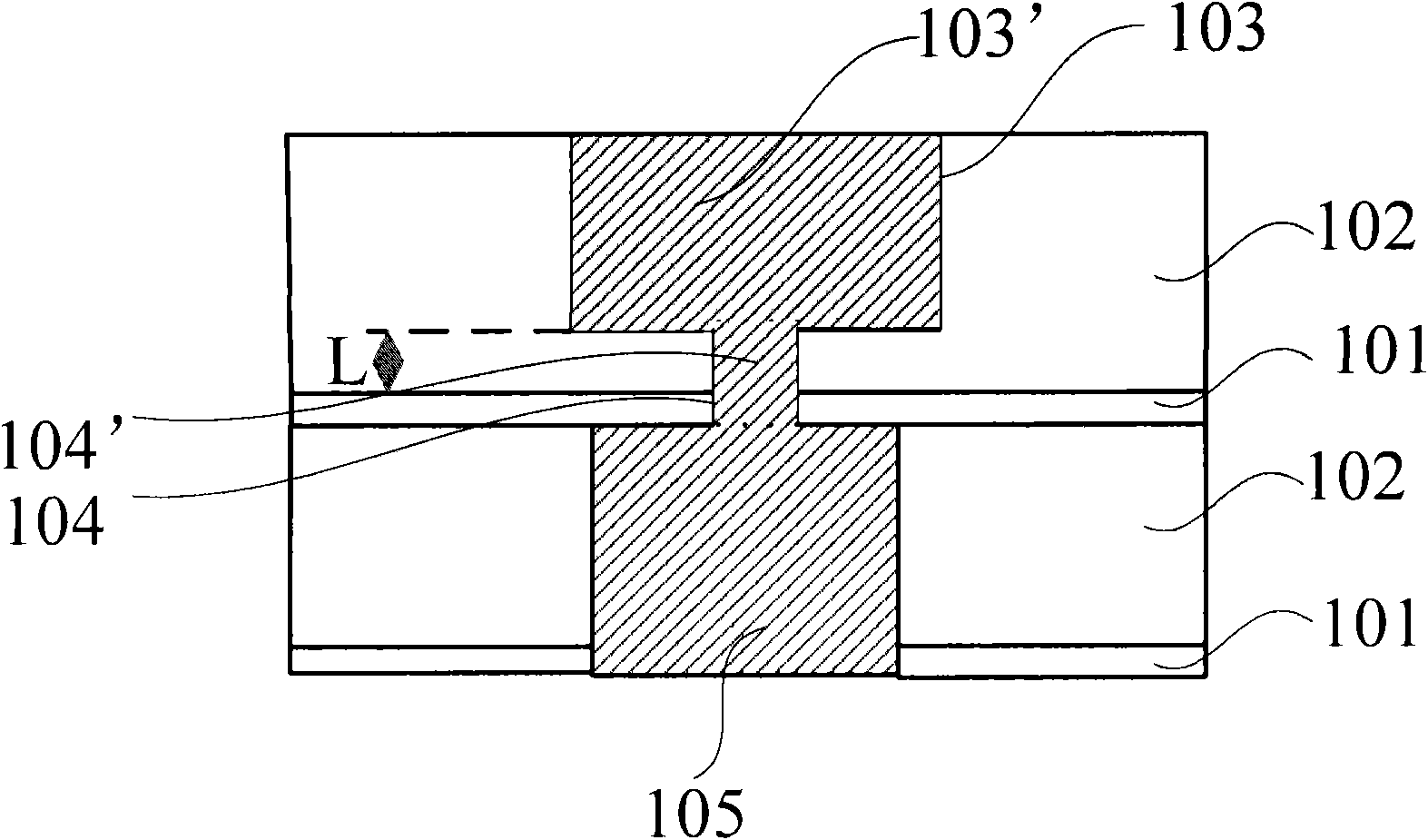
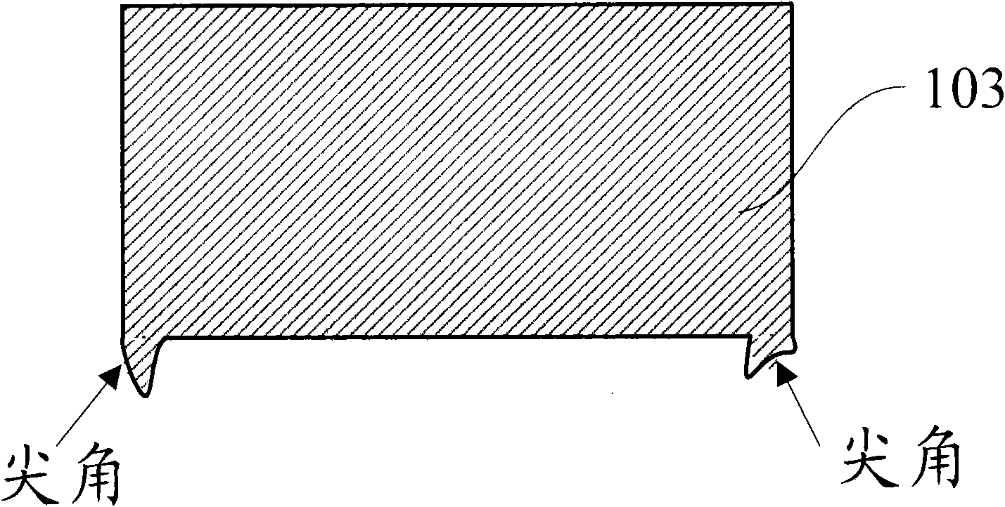
[0033] The present invention has been described in detail using schematic diagrams. When describing the embodiments of the present invention in detail, for the convenience of explanation, the schematic diagram showing the structure will not be partially enlarged according to the general scale, which should not be used as a limitation of the present invention. In addition, in actual production In , the three-dimensional space dimensions of length, width and depth should be included.

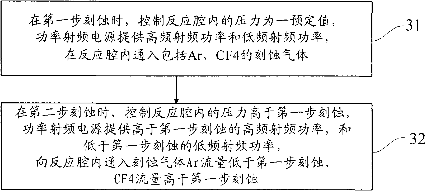
[0034] The main etching adopts a two-step etching method. The first etching is basically the same as the existing technology, but the etching time is shortened. In the second etching step, various etching process parameters are adjusted to effectively eliminate The purpose...


PUM


Abstract

The method discloses a method for etching a groove. In the invention, the etching is carried out in a reaction chamber, and the method comprises the a following main etching step implemented by two steps: 1, etching on the basis of the original process parameters; and 2, etching on the basis of the regulated process parameters. By adopting the method, micro grooves can be effectively eliminated to further reduce the RC delay.

Description

technical field [0001] The invention relates to the etching field of semiconductor manufacturing technology, in particular to a method for etching grooves. Background technique [0002] At present, in the back-end process of semiconductor devices, multiple layers of metal interconnection layers can be provided according to different needs, and each layer of metal interconnection layers includes metal interconnection lines and insulating layers, which requires the manufacture of grooves and connections for the above-mentioned insulating layers. Holes, and then deposit metal in the above-mentioned grooves and connection holes, the deposited metal is the metal interconnection, and copper is generally selected as the material of the metal interconnection. figure 1 It is a schematic cross-sectional view of a part of the copper interconnection layer in the prior art: a trench 103 and a connection hole 104 are etched on an insulating layer including an etch stop layer 101 and a sil...

Claims


Application Information

Patent Timeline
Patent Type & Authority Applications(China)
IPC IPC(8): H01L21/311H01L21/768
Inventor 孙武李若园
Owner SEMICONDUCTOR MANUFACTURING INTERNATIONAL (BEIJING) CORP
Why Eureka
Try Eureka