Semiconductor high-voltage device chip and manufacture method thereof

A high-voltage device and semiconductor technology, applied in the field of semiconductor high-voltage device chips, can solve the problems of increasing grooves, limiting the depth of grooves, and long diffusion time of diffusion temperature, so as to improve heat dissipation capacity, increase breakdown voltage, and reduce the difficulty of scribing Effect

Inactive Publication Date: 2010-10-20
JIANGSU JIEJIE MICROELECTRONICS
View PDF0 Cites 10 Cited by
  • Summary
  • Abstract
  • Description
  • Claims
  • Application Information

AI Technical Summary

Problems solved by technology

There are two disadvantages: First, because the lateral diffusion of through-isolation diffusion is very wide, it occupies a lot of silicon wafer area, making the utilization rate of silicon wafers low; second, the diffusion depth of through-isolation diffusion is very deep, which needs to be larger than that of a silicon single wafer One-half of the thickness requires a very high diffusion temperature and diffusion time. The thicker the silicon single wafer, the higher the diffusion temperature and the longer the diffusion time is required. During the high temperature and long-term diffusion process, a large amount of Structural defects reduce the pass rate
However, since the grooves on the front and back are symmetrical in position, when the thickness of the silicon wafer is constant, the depth of the groove cannot be deepened, such as image 3 Shown: Let the thickness of the silicon wafer be t, the depth of the groove be d, and the thickness between the two grooves be W. To ensure that the silicon wafer is less broken during the manufacturing process, W must be greater than 100um, so that d≤1 / 2(t- 100um), when the thickness of the silicon wafer is constant, the maximum value of the groove depth dmax=1 / 2t-50um, even so, the silicon wafer is still very easy to break during the process
The disadvantages of this technology are: the depth of the trench is limited, which is not conducive to higher voltage; the silicon wafer is easily broken during the manufacturing process; under a certain breakdown voltage requirement, due to the insufficient depth of the trench, the width of the trench needs to be increased. The area of ​​the soldering area on the back of the chip is reduced, which is not conducive to heat dissipation; the dicing needs to be cut on the glass layer, the speed is very slow (6-8mm / sec), and it is easy to cause the chip to crack and produce waste products

Method used


Image

  • Semiconductor high-voltage device chip and manufacture method thereof
  • Semiconductor high-voltage device chip and manufacture method thereof
  • Semiconductor high-voltage device chip and manufacture method thereof

Examples


Embodiment Construction

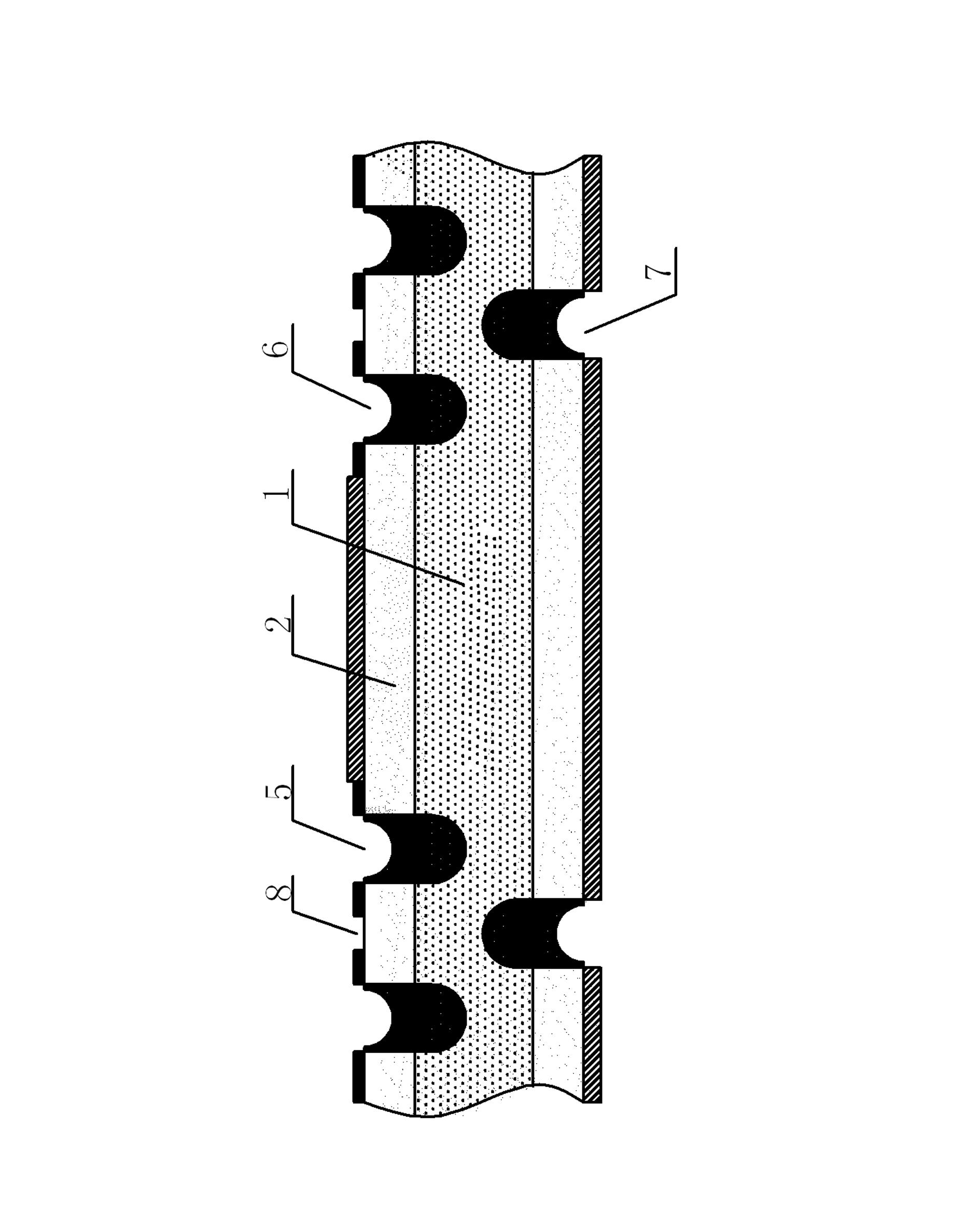
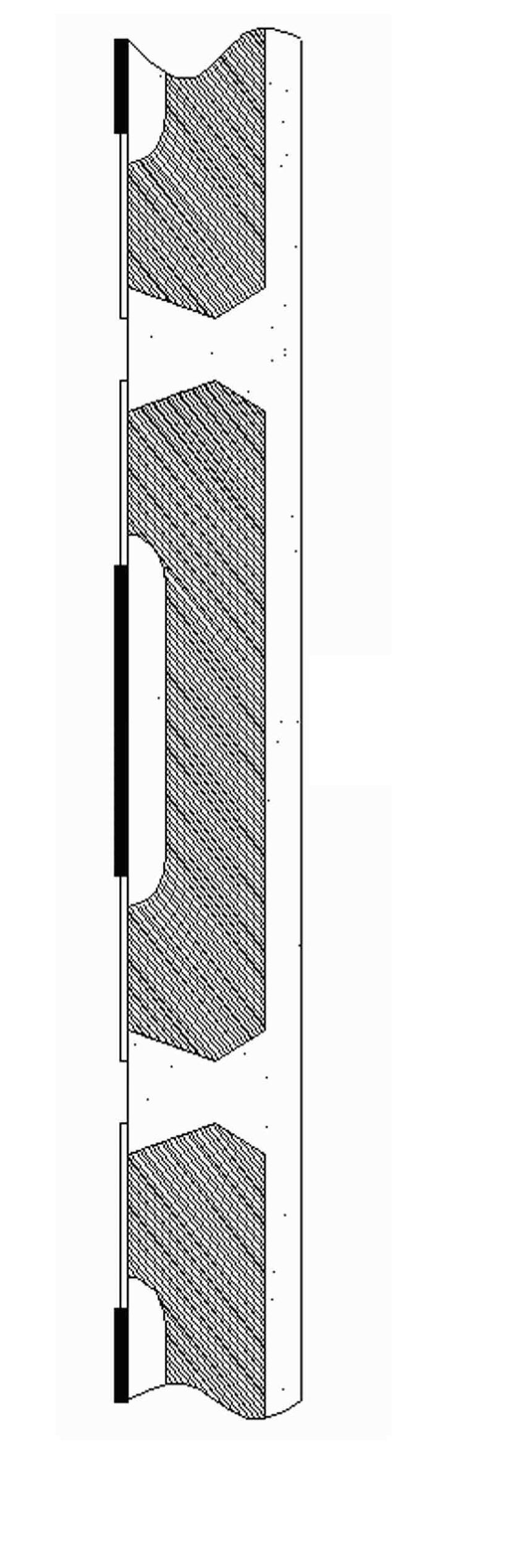
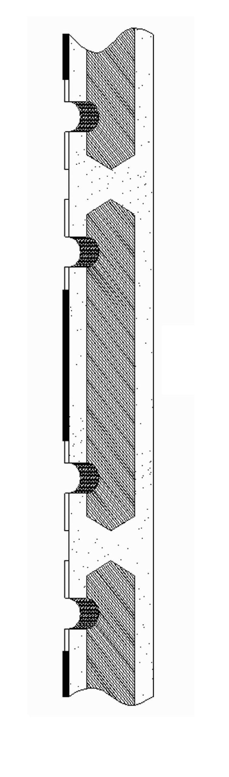
[0027] Such as Figures 4 to 6 As shown, the semiconductor high-voltage device chip includes a silicon single wafer 1, a front P-type diffusion layer 2 formed in the silicon single wafer 1, a back P-type diffusion layer 3, and a front internal annular groove 6 with a width of 100-400um. The half-width of the outer groove 7 inside the back is 90-260um, the depth of the groove is 80-200um, the inner groove 6 and the outer groove 7 are arranged asymmetrically in the longitudinal direction, and a width of 90mm is left between the chips on the front. - 110um spacer zone 8, the side walls and bottom surfaces of the inner groove 6 and the outer groove 7 are covered with an oxygen-doped semi-insulating polysilicon passivation film 4 with a thickness of 1.3-1.8um, and an oxygen-doped semi-insulating polysilicon passivation film 4 is covered with a glass protective film 5 with a thickness of 40-60um.

[0028] The present invention produces the method for semiconductor high-voltage devi...


PUM

PropertyMeasurementUnit
Widthaaaaaaaaaa
Thicknessaaaaaaaaaa
Groove depthaaaaaaaaaa

Abstract

The invention relates to a semiconductor high-voltage device chip. An inner groove and an outer groove of a chip are asymmetrically arranged in the longitudinal direction, an interval zone is reserved between a front chip and the chip, a layer of oxygen-doped semi-insulating polycrystalline silicon passivating film covers the side walls and the surfaces of the bottoms of the inner groove and the outer groove, and a layer of glass protective film covers on the oxygen-doped semi-insulating polycrystalline silicon passivating film. The invention also relates to a manufacture method of the semiconductor high-voltage device chip, which comprises the steps of: asymmetrically arranging the inner groove and the outer groove in the longitudinal direction in the step of corroding the front face and the back face while carrying out a wet method, reserving the interval zone between the front chip and the chip; and depositing an SIPOS (Semi-insulation Polycrystalline Silicon) film and a glass passivating film between the step of corroding the front face and the back face while carrying out the wet method and the step of evaporating an aluminum film at the front face. The invention has the advantages of capability of directly improving the breakdown voltage, lowering the breaking ratio of a silicon chip in the manufacture, improving the heat radiating capacity, reducing the cutting-up difficulty, enhancing the cutting-up speed, having no crack phenomenon after cutting-up, and increasing the reliability of the device.

Description

technical field [0001] The invention relates to a semiconductor device chip, in particular to a semiconductor high-voltage device chip. [0002] The invention also relates to a method for manufacturing the semiconductor high-voltage device chip. Background technique [0003] There is a class of semiconductor devices (such as thyristors) that require two breakdown voltages, forward and reverse, V DRM and V RRM The chip of this type of device needs to make two symmetrical and opposite P-N junctions on the front and back sides of the same silicon chip. The breakdown voltage value of the two P-N junctions is required to be high, generally reaching 600V ~ 2400V In order to meet the requirements of use. [0004] There are three commonly used chip manufacturing technologies for such devices: [0005] A. Planar technology: communication isolation diffusion plus planar terminal structure, see figure 1 ; [0006] B. Single mesa technology: through isolation diffusion plus front ...

Claims


Application Information

Patent Timeline
IPC IPC(8): H01L29/74H01L21/332H01L21/31H01L21/306
CPCH01L23/3178
Inventor 王成森黎重林王琳薛治祥颜呈祥
Owner JIANGSU JIEJIE MICROELECTRONICS
Why Eureka
Try Eureka