Supercharge Your Innovation With Domain-Expert AI Agents!

OTP (One Time Programming) device and manufacture method

A device and active area technology, applied in semiconductor/solid-state device manufacturing, electric solid-state devices, semiconductor devices, etc., can solve the problems of OTP programming capability limitation, waste of memory cell area, affecting coupling capacitor voltage coupling efficiency, etc. The effect of hot electron generation ability, improving programming ability

Active Publication Date: 2010-11-03
SHANGHAI HUAHONG GRACE SEMICON MFG CORP
View PDF0 Cites 2 Cited by
  • Summary
  • Abstract
  • Description
  • Claims
  • Application Information

AI Technical Summary

Problems solved by technology

This depletion layer capacitance is much smaller than the gate oxide capacitance, and it is connected in series with the gate oxide capacitance during programming, which greatly affects the voltage coupling efficiency of the coupling capacitor.
Therefore, in order to ensure programming efficiency, the area of ​​the capacitive coupling part of the common OTP structure will be large, wasting the area of ​​the memory cell; and usually require a higher programming pulse voltage to reduce the voltage loss during capacitive coupling. It is bound to put forward higher requirements for the process
[0006] In addition, the general process will use high-energy, low-concentration LDD implantation in the transistor area to prevent CHE from affecting the reliability of the transistor. Hot electron injection (HCI, hot carrier injection), which is a limitation on the programming ability of OTP itself

Method used


Image

  • OTP (One Time Programming) device and manufacture method
  • OTP (One Time Programming) device and manufacture method
  • OTP (One Time Programming) device and manufacture method

Examples


Embodiment Construction

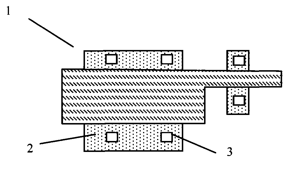
[0026] Such as Figure 5 As shown, the preparation method of OTP device of the present invention comprises the following steps, and concrete structural diagram is as shown in Figure 6, and in Figure 6, left column is the transistor part of OTP device, and right column is coupling capacitance part:

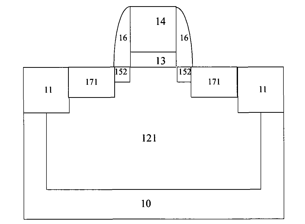
[0027] First, if Figure 6A As shown, effectively isolated well and field regions are formed on the substrate. In the transistor part, the P well region 121 and the field region 11 are formed on the substrate 10 , and in the coupling capacitor part, the N well region 122 and the field region 11 are formed on the substrate 10 .

[0028] Then, if Figure 6B As shown, a gate oxide layer 13 is formed above the active regions of the transistor and the coupling capacitor, and polysilicon 14 is formed on the gate oxide layer 13 . After that, etch the polysilicon floating gate forming the transistor and the coupling capacitor to form a Figure 6C the structure shown;

[0029] Next, if...


PUM


Abstract

The invention discloses a manufacture method of an OTP (One Time Programming) device, which comprises the following steps of: 1, forming a well region and a field region which are effectively isolated on a substrate; 2, forming a gate oxide layer above an active area, forming polysilicon on the gate oxide layer and etching to form a transistor polysilicon floating gate; 3, carrying out light dope leakage implantation on the active area firstly; 4, carrying out low-energy high-dosage implantation on the active area in a transistor part; and 5, forming a polysilicon side wall on the side face of the polysilicon gate, and then forming an active area of a NMOS (N-channel Metal Oxide Semiconductor) / PMOS (P-channel Metal Oxide Semiconductor) transistor by using an ion implantation technology. The invention also discloses an OTP device, and a P+ active area and a N+ active area of a coupling capacitor part are arranged below the polysilicon floating gate. The invention can improve the programming efficiency and effectively reduce a storage area.

Description

technical field [0001] The invention relates to the field of semiconductor integrated circuits, in particular to an OTP device and a preparation method of the OTP device. Background technique [0002] OTP (One Time Programming, one-time programmable) device is a storage device. Compared with multiple programming, its programming process is an irreversible activity. It is suitable for applications where the program is fixed because the cost is relatively low. low and widely used. [0003] Such as Figure 1a As shown, the existing OTP device generally consists of a coupling capacitor NMOS capacitor plus an NMOS transistor. Such as Figure 1b As shown, the layout of the OTP device in the prior art includes polysilicon, N+ active regions, and contacts. Usually the OTP device implements the basic programming and charge storage functions of the OTP through a transistor and a floating gate capacitor. [0004] The working principle of the existing OTP device is to use FN tunneli...

Claims


Application Information

Patent Timeline
IPC IPC(8): H01L21/8247H01L21/265H01L27/115H01L29/788H01L29/06
Inventor 胡晓明蔡明祥苗彬彬
Owner SHANGHAI HUAHONG GRACE SEMICON MFG CORP
Features
  • R&D
  • Intellectual Property
  • Life Sciences
  • Materials
  • Tech Scout
  • Unparalleled Data Quality
  • Higher Quality Content
  • 60% Fewer Hallucinations
Learn More