Antenna for ic tag and method of manufacturing the same

A manufacturing method and antenna technology, applied to recording carriers used in machines, metal/alloy conductors, and structural forms of radiation elements, etc., can solve problems such as slow printing speed, difficulty in forming a coating, hindering IC label productivity, and cost competitiveness. , to achieve the effect of reducing manufacturing cost and reducing surface roughness

Inactive Publication Date: 2010-11-17
PROVIDENT
View PDF5 Cites 20 Cited by
  • Summary
  • Abstract
  • Description
  • Claims
  • Application Information

AI Technical Summary

Problems solved by technology

[0011] However, in order to obtain a desired volume resistance value, the film thickness of the IC tag antenna formed using the above-mentioned conventional conductive paste must be several μm to several tens of μm (after drying). On the material, it is necessary to perform a drying process at a temperature above 100°C for several minutes to tens of minutes.
Therefore, the above-mentioned operation becomes the bottleneck of the processing operation, and there is a problem that it hinders the improvement of productivity and cost competitiveness for IC tags.
[0012] In addition, in the process of manufacturing (printing) the above-mentioned conventional IC tag antenna, a printing method with a relatively slow printing speed, that is, a flat silk screen print (printing speed: 1 to 2m / min), or rotary silk screen print (printing speed: 5-20m / min), in the above-mentioned screen printing method, even if the finest screen mesh is used, the screen The mesh thickness is also about 20 μm or more, but there is still a problem that it is difficult to form a film with a film thickness of 5 μm or less

Method used


Image

  • Antenna for ic tag and method of manufacturing the same
  • Antenna for ic tag and method of manufacturing the same
  • Antenna for ic tag and method of manufacturing the same

Examples


Embodiment 1

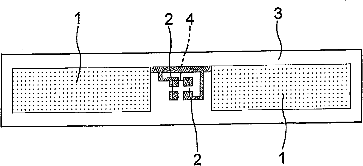
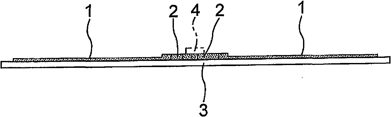
[0068] In this example, the IC tag antennas [Example 1] to [Example 3] and [Comparative Example 1] and [Comparative Example 2] prepared by flexographic printing using water-based conductive ink were used. Antennas for IC tags [Comparative Example 3] prepared by screen printing with ink, and conventional antennas for IC tags [Comparative Example 4] prepared by etching aluminum foil, compared the antenna section 1 of the antenna for IC tags above. thickness (μm), volume resistance value (resistivity: Ω·cm) of the antenna unit 1, and the like.

[0069] In Examples 1 to 3 and Comparative Examples 1 and 2, the following aqueous conductive ink (low-temperature sintered nano silver conductive ink) and substrates were used.

[0070] nano silver ink

[0071] A: TEC-PR-030 manufactured by InkTec Co., Ltd. (Korea)

[0072] Composition Silver particles - average particle size: 20-50μm Content rate: 40wt% or less

[0073] Binder (organic complex compound) content rate - 35wt% or less ...

Embodiment 2

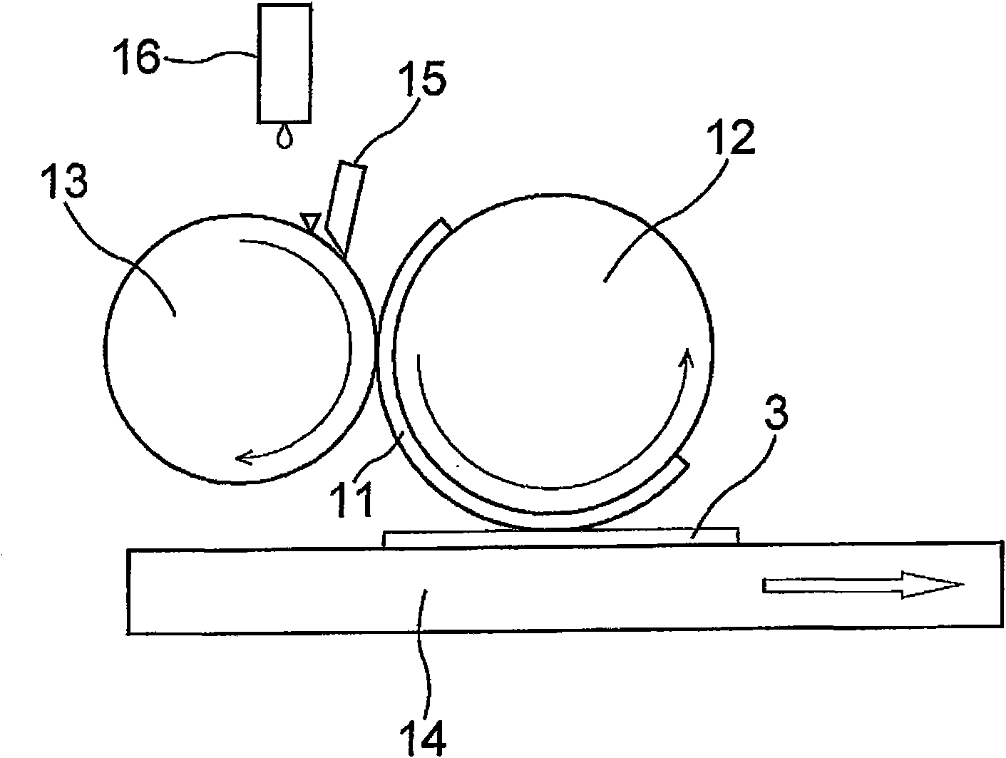
[0107] Use ink retention of 0.3ml / m 2 The printing plate of the above-mentioned flexographic printing machine was used to print and transfer the ink A to the PET substrate, and after drying at 120° C. for 2 minutes, the IC tag antenna of Example 2 was obtained.

Embodiment 3

[0109] The ink holding capacity of the antenna part is 1.5ml / m 2 , The ink holding capacity of the chip connection part is 3.0ml / m 2 The printing plate of the above-mentioned flexographic printing machine was used to print and transfer the ink A to the PET substrate, and after drying at 120° C. for 2 minutes, the IC tag antenna of Example 3 was obtained.


PUM

PropertyMeasurementUnit
particle sizeaaaaaaaaaa
thicknessaaaaaaaaaa
thicknessaaaaaaaaaa

Abstract

The invention provides an antenna for IC tag that has small membrane thickness than the prior products and can reach the necessary low resistance of the non-contact type storage medium, and method of manufacturing the antenna for IC tag at low cost efficiently. A film shape conductive film antenna with specified circuit pattern is formed on the surface of the substrate (3) by using the aqueous conductive ink containing silver particles, adhesive and water, the conductive film antenna includes an antenna part (1) for transmitting and receiving the electromagnetic wave, and an interconnecting piece (2) connected to the IC chip (4).

Description

technical field [0001] The present invention relates to an antenna mounted in a non-contact storage medium such as an IC tag or an IC card exchanging information by wireless communication, and a manufacturing method thereof. Background technique [0002] In recent years, IC cards, etc., which can read and rewrite information in a non-contact manner by wireless communication, have been promoted instead of contact storage media such as cash cards and credit cards partially embedded with magnetic tapes. In addition, a small IC tag consisting of only a communication circuit (antenna) and an IC chip that undertakes the communication and storage functions of the IC card has been proposed. RFID (Radio Frequency IDentification: radio frequency identification) system of IC tags. [0003] At present, there are two methods for identifying and rewriting non-contact storage media such as the above-mentioned IC card and IC tag (RFID tag), the electromagnetic induction method and the radi...

Claims


Application Information

Patent Timeline
Patent Type & Authority Applications(China)
IPC IPC(8): H01Q1/38H01B1/02G06K19/077
CPCG06K19/077H01Q1/38
Inventor 坂梨孝一
Owner PROVIDENT
Why Eureka
Try Eureka