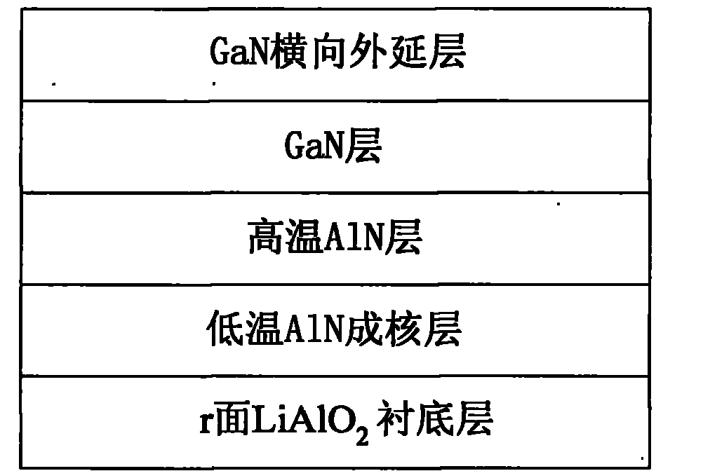
MOCVD growth method of non-polar m-surface GaN based on gamma-surface LiAlO2 substrate
A non-polar, substrate technology, applied in the field of microelectronics, can solve the problems of poor surface morphology and poor crystal quality, and achieve the effect of improving surface morphology and crystal quality
- Summary
- Abstract
- Description
- Claims
- Application Information
AI Technical Summary
Problems solved by technology
Method used
Image

Examples
Embodiment 1
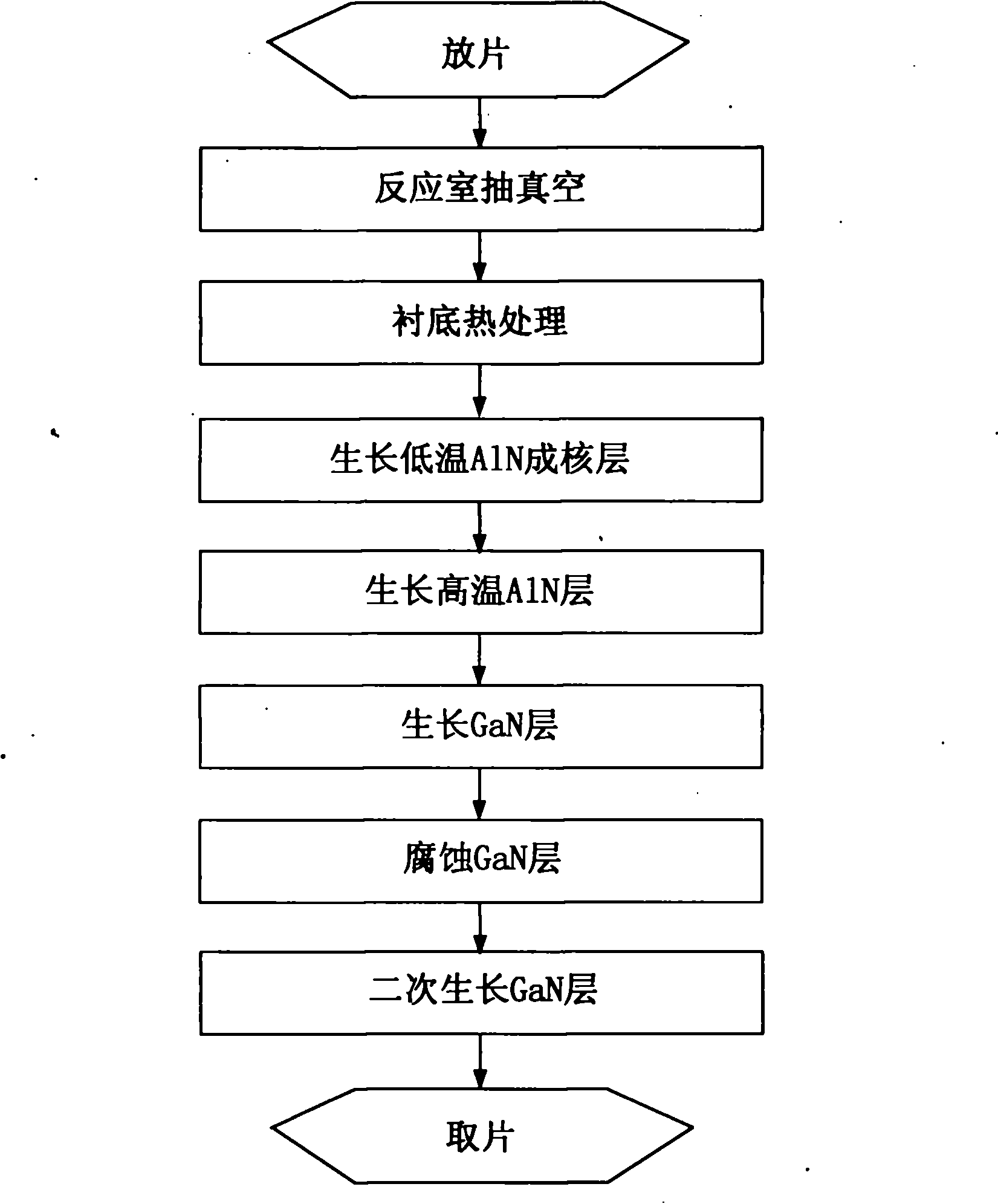
[0020] The realization steps of the present invention are as follows:
[0021] Step 1, performing heat treatment on the substrate.
[0022] γ-surface LiAlO 2 The substrate substrate is placed in the metal organic chemical vapor deposition MOCVD reaction chamber, and hydrogen gas is introduced into the reaction chamber, and the vacuum degree in the reaction chamber is less than 2×10 -2 Torr, the substrate heating temperature is 900° C., the time is 4 minutes, and the reaction chamber pressure is 40 Torr, the substrate is heat-treated.
[0023] Step 2, growing a 550°C low-temperature AlN nucleation layer.
[0024] Lower the temperature of the substrate after the heat treatment to 550°C, feed the aluminum source with a flow rate of 20 μmol / min, hydrogen gas with a flow rate of 1200 sccm and ammonia gas with a flow rate of 1500 sccm into the reaction chamber, and grow a thickness of 40 nm under the condition of maintaining a pressure of 40 Torr low temperature AlN nucleation la...
Embodiment 2
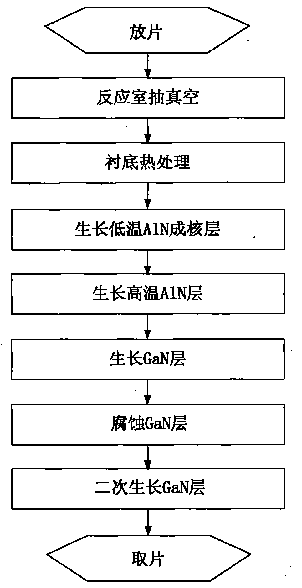
[0036] The realization steps of the present invention are as follows:
[0037] Step A, performing heat treatment on the substrate.
[0038] m-plane LiAlO 2 The substrate substrate is placed in the metal organic chemical vapor deposition MOCVD reaction chamber, and the mixed gas of hydrogen and ammonia is introduced into the reaction chamber, and the vacuum degree in the reaction chamber is less than 2×10 -2 Torr, the heating temperature of the substrate substrate is 800° C., the time is 3 minutes, and the reaction chamber pressure is 10 Torr, the substrate substrate is heat-treated.
[0039] Step B, growing a 500°C low-temperature AlN nucleation layer.
[0040]Lower the temperature of the heat-treated substrate to 500°C, feed the aluminum source with a flow rate of 10 μmol / min, hydrogen gas with a flow rate of 1200 sccm, and ammonia gas with a flow rate of 1000 sccm into the reaction chamber, and grow the thickness under the condition of maintaining a pressure of 10 Torr A ...
Embodiment 3
[0052] The realization steps of the present invention are as follows:
[0053] Step 1: performing heat treatment on the base substrate.
[0054] γ-surface LiAlO 2 The substrate substrate is placed in the metal organic chemical vapor deposition MOCVD reaction chamber, and hydrogen gas is introduced into the reaction chamber, and the vacuum degree in the reaction chamber is less than 2×10 -2 Torr, the heating temperature of the substrate substrate is 1000° C., the time is 5 minutes, and the reaction chamber pressure is 700 Torr, the substrate substrate is heat treated.
[0055] Step 2, growing a 600°C low-temperature AlN nucleation layer.
[0056] Lower the temperature of the heat-treated substrate to 600°C, feed the aluminum source with a flow rate of 120 μmol / min, hydrogen gas with a flow rate of 1200 sccm and ammonia gas with a flow rate of 10000 sccm into the reaction chamber, and grow the thickness under the condition of maintaining a pressure of 700 Torr A low temperatu...
PUM
| Property | Measurement | Unit |
|---|---|---|
| Thickness | aaaaa | aaaaa |
| Thickness | aaaaa | aaaaa |
| Thickness | aaaaa | aaaaa |
Abstract
Description
Claims
Application Information