Wide-spectrum medium short wave infrared Dewar window based on silicon substrate and preparation process

A wide-spectrum, silicon-based technology, applied in optics, optical components, instruments, etc., can solve the problems of metallization process research difficulties, absorption affecting channel optical efficiency, etc., to eliminate the influence of water vapor absorption, improve reliability, and stabilize product performance Effect

Inactive Publication Date: 2011-11-02
SHANGHAI INST OF TECHNICAL PHYSICS - CHINESE ACAD OF SCI
View PDF0 Cites 0 Cited by
  • Summary
  • Abstract
  • Description
  • Claims
  • Application Information

AI Technical Summary

Problems solved by technology

In this invention, the window substrate is silicon, and there are great difficulties in the research on the metallization process of the silicon substrate and the wide-spectrum anti-reflection coating of 1.2-4.8um.
First of all, this spectral band includes 2.7-2.9um, the water vapor absorption that exists in most fluoride and oxide low-refractive index materials, and this is just an important imaging channel for mid-short-wave infrared imagers, which cannot be well resolved. Absorption issues will seriously affect the optical efficiency of this channel

Method used


Image

  • Wide-spectrum medium short wave infrared Dewar window based on silicon substrate and preparation process
  • Wide-spectrum medium short wave infrared Dewar window based on silicon substrate and preparation process
  • Wide-spectrum medium short wave infrared Dewar window based on silicon substrate and preparation process

Examples


Embodiment Construction

[0024] The specific implementation manners of the present invention will be further described in detail below in conjunction with the accompanying drawings.

[0025] The concrete technical index requirement of the embodiment of the present invention is:

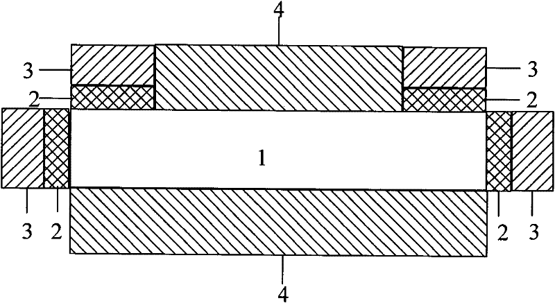
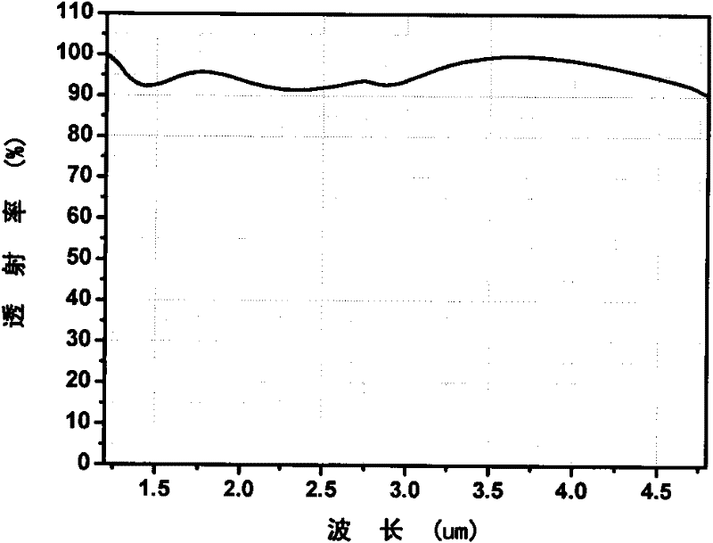
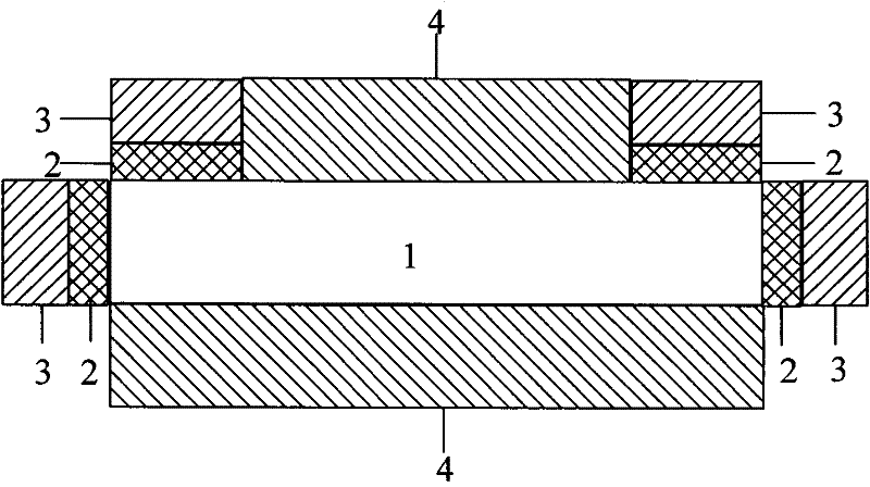
[0026] 1.2-4.8um, the average transmittance is greater than 93%; the thickness of the metallization layer is greater than 1um; the base material is silicon.

[0027] According to the technical requirements and the physical characteristics of various thin films, first determine the development sequence of each part. Since the metallization process requires the process of mask protection and mask removal, in order to prevent the performance of the infrared dielectric film from being affected, it is necessary to perform metallization first. After the metallization is completed, the gold layer is fully aged to carry out the development of the next step of the dielectric anti-reflection coating.

[0028] Considering the influenc...


PUM

PropertyMeasurementUnit
thicknessaaaaaaaaaa
transmittivityaaaaaaaaaa

Abstract

The invention discloses a wide-spectrum medium short wave infrared window for detector / Dewar packaging and welding and a preparation process. The window takes silicon as the substrate material. The edges and the side of one surface of the window are plated with gold films in certain thickness, with a nanoscale nickel-chromium layer as the bonding layer. The gold films are called metalization layer, and the edges and the side are used for detector / Dewar packaging and welding. The middle areas of the surface and the other surface are plated with wide-spectrum medium short wave infrared antireflection films with multilayer film structure and alternate high / low refractive indexes, wherein the antireflection films take ZnS and YF3 as the materials with high / low refractive indexes and the equivalent layer adopts ZnS and Si. The antireflection films are plated by such specific processes as ion source assistance, appropriate substrate temperature, etc. The average transmissivity T of the window is more than 95% in the range of 1.2-4.8mu m and the water-vapor absorption peak commonly appearing on YF3 does not appear on the window in the range of 2.7-3.0mu m. The patented product is stable in performance and is suitable for the medium short wave infrared detectors / Dewar of the modern multi-spectrum space remote sensing instruments.

Description

technical field [0001] This patent relates to optical thin-film components, specifically a silicon-based, wide-spectrum short-wave infrared metallized window with high transmittance, which is suitable for sealing and welding with the detector Dewar window frame. technical background [0002] The optical window is an important part of the imaging optical system. In order to ensure the reliability of the package between the window and the detector Dewar window frame, the metallization layer must have high reliability. At the same time, to ensure the optical efficiency of the system, an anti-reflection coating with high transmittance and high reliability is required. [0003] In the existing Dewar windows, the substrates are mostly Ge and gemstones, and the wavelength bands are relatively narrow. The metal layer is a 300-400 Angstrom chromium layer plus a 1um thick gold layer. Such a process cannot meet the requirements for the use of Dewar windows in short- and medium-wavele...

Claims


Application Information

Patent Timeline
Patent Type & Authority Patents(China)
IPC IPC(8): G02B1/11G02B1/115
Inventor 于天燕梁俊华秦杨章卫祖刘定权
Owner SHANGHAI INST OF TECHNICAL PHYSICS - CHINESE ACAD OF SCI
Why Eureka
Try Eureka