
High-power planar junction bidirectional TVS diode chip and production method thereof

A production method and planar junction technology, applied in the direction of electrical components, circuits, semiconductor devices, etc., can solve the problems of reduced product lifetime, low effective utilization rate of silicon wafers, and impact on product reliability, so as to avoid the stress of glass passivation film , short production process and high reliability

Inactive Publication Date: 2010-12-15
NANTONG MINICHIP MICRO ELECTRONICS
View PDF5 Cites 21 Cited by
  • Summary
  • Abstract
  • Description
  • Claims
  • Application Information

AI Technical Summary

Problems solved by technology

The more advanced technology in the manufacture of TVS diode chips today is to use a low-resistivity N-type double-milled single wafer for preparation. The process steps are: pickling, cleaning, diffusion, groove, glass passivation, chemical plating, alloying , electroless plating, steam gold, testing, scribing, and splitting. The disadvantage of this method is that the product production process includes two diffusions, one is N+ type diffusion, and the other is P type diffusion. Since the product is a mesa junction structure , so it is deep junction diffusion, the diffusion time is long, the minority carrier life of the product is reduced, and the silicon wafer is easy to warp, causing fragments, and inconvenient to operate; the electrode of the product is formed by electroless plating, which requires two coatings, and to ensure the product The reliability of the plating layer must be covered with a layer of gold (Aμ) film, the process is complicated; the protection of the PN junction adopts the method of digging grooves and glass passivation, and the process flow is long; directly scribing on the glass passivation layer will affect the quality of the product. Reliability; the product adopts mesa technology, the effective utilization rate of silicon wafer is low, and the production cost is high

Method used


Image

  • High-power planar junction bidirectional TVS diode chip and production method thereof
  • High-power planar junction bidirectional TVS diode chip and production method thereof

Examples


Embodiment Construction

[0027] Select an N-type silicon double-grinding chip with a resistivity of 0.01-0.02Ω.cm and a thickness of 225-235 μm, and produce a high-power planar junction bidirectional TVS diode chip according to the following method:

[0028] 1) Silicon wafer cleaning: Use No. 1 electronic cleaning solution (NH 4 OH:H 2 o 2 :H 2 The volume ratio of O is 1:2:5) and No. 2 electronic cleaning solution (HCL:H 2 o 2 :H 2 The volume ratio of O is 1:2:6) for cleaning, the reaction temperature of the cleaning solution is 85±5°C, the reaction time is 10 minutes, rinse with deionized water (resistivity greater than 14MΩ.cm) for 30 minutes, and dry.

[0029] 2) Oxidation: Put the silicon wafer on the carrier boat, push it into the diffusion furnace, raise the temperature to 1150±5°C, and 2 and O 2 The first oxidation is carried out in the mixed gas composed of 2 、H 2 and O 2 The second oxidation is carried out in the mixed gas, the time is 240±5 minutes, and then in N 2 and O 2 Carry ...


PUM


Abstract

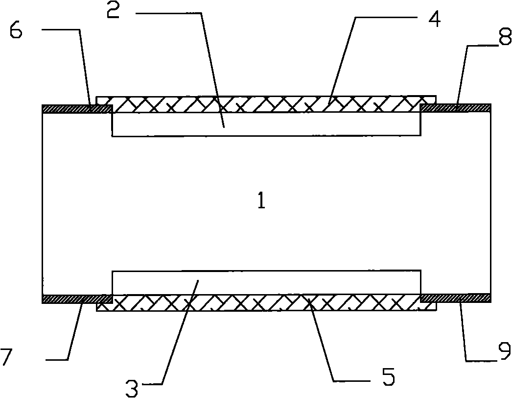
The invention discloses a high-power planar junction bidirectional TVS diode chip and a production method thereof, and relates to the technical field of manufacturing of a semiconductor device. The production method comprises the following steps of: protecting both surfaces of a silicon wafer with SiO2; photo-etching diffusion windows on the both surfaces; simultaneously forming P-type diffusion regions in the diffusion windows; and forming coated regions on the surfaces of the P-type diffusion regions. By adopting shallow junction diffusion, the process has the advantages of short diffusion time, long product life, high performance, no warping of the silicon wafer and low fragmentation rate of the product. Trenching is not needed during the production, so the utilization ratio of the silicon wafer and the current density of the product can be improved. Scribing is not performed on a glass passivation layer, so the stress of a glass passivation film can be prevented so as to contribute to ensuring firm structure, reducing leakage current, particularly the leakage current at the high temperature and improving the reliability of the product. By using a multilevel metallization mode, the coating can be finished at one time and has simple process and high reliability.

Description

technical field [0001] The invention relates to the technical field of manufacturing semiconductor devices, in particular to a method for preparing a high-power planar junction bidirectional TVS diode. Background technique [0002] For a long time, in the field of semiconductor device manufacturing, people have made unremitting efforts in terms of structural design, cost reduction, reliability, and improvement of product cost performance. The more advanced technology in today's TVS diode chip manufacturing is to use a low-resistivity N-type double-grinding single wafer for preparation. The process steps are: pickling, cleaning, diffusion, groove, glass passivation, chemical plating, alloying , electroless plating, steam gold, testing, scribing, and splitting. The disadvantage of this method is that the product production process includes two diffusions, one is N+ type diffusion, and the other is P type diffusion. Since the product is a mesa junction structure , so it is a d...

Claims


Application Information

Patent Timeline
IPC IPC(8): H01L29/861H01L21/329
Inventor 周明苏学杰穆连和顾理健
Owner NANTONG MINICHIP MICRO ELECTRONICS
Learn More