Nano-tubes semiconductor device and preparation method thereof

A semiconductor and device technology, which is applied in the field of nanotube vertical channel metal oxide silicon field effect transistor semiconductor devices, can solve the complex and expensive processing technology of shielded gate structure transistors, reduce the switching speed of shielded gate structure transistors, increase the Drain-source "on" impedance variation range and other issues to achieve the effect of improving conversion performance, reducing parasitic capacitance, and high conversion speed

Active Publication Date: 2010-12-22
ALPHA & OMEGA SEMICON INT LP
View PDF4 Cites 18 Cited by
  • Summary
  • Abstract
  • Description
  • Claims
  • Application Information

AI Technical Summary

Problems solved by technology

Shielded gate structure transistors have low gate-drain capacitance (Cgd), but due to the non-self-aligning nature of the gate oxide and N-drift region overlap, shielded gate structure transistor devices increase the drain-source "on" resistance (Rdson) range of variation
In addition, the unit step process of polysilicon electrode, interpolysilicon dielectric (IPD) and channel etching (side wall angle) makes the processing technology of shielded gate structure transistor complex and expensive
Also, the increase in output capacitance and shielded gate polysilicon resistance reduces the switching speed of shielded gate structure transistors

Method used


Image

  • Nano-tubes semiconductor device and preparation method thereof
  • Nano-tubes semiconductor device and preparation method thereof
  • Nano-tubes semiconductor device and preparation method thereof

Examples


no. 1 example

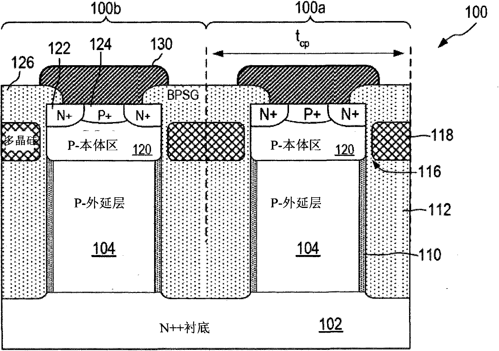
[0081] figure 1 It shows a cross-sectional view of a vertical channel metal oxide silicon field effect transistor device according to a first embodiment of the present invention. see figure 1 , an N-type vertical channel MOSFET device ("NMOS transistor") 100, formed in an array of parallel transistor cells 101a and 101b. A certain number of transistor cells are used to form an array to obtain an NMOS transistor 100 with certain breakdown voltage and Rdson (drain-source "on" resistance) characteristics. Transistor arrays can be one-dimensional or two-dimensional arrays, depending primarily on the number of transistor cells included. For example, a striped unit cell structure can use a one-dimensional array, and a hexagonal unit cell structure can use a two-dimensional array, as described in further detail below.

[0082] The NMOS transistor 100 is formed on an N++ substrate 102 with a relatively high doping concentration. The N++ substrate 102 serves as the drain electrode ...


PUM


Abstract

The invention relates to a semiconductor device and a preparation method thereof. A nano-tubes area is produced by adopting the thin epitaxial layer formed on the channel sidewall of the semiconductor body. The thin epitaxial layer possesses an even and consistent dosage concentration. A first thin epitaxial layer in the same conducting type as the semiconductor body is formed on the channel sidewall of the semiconductor body. A second thin expitaxial layer in the opposite conducting type with the semiconductor body is formed on a first expitaxial layer. The first and the second expitaxial layer possess an even and consistent dosage concentration. An electric charge balance is achieved by choosing an appropriate first and second expitaxial layer and appropriate thickness and dosage concentration of the semiconductor body. The semiconductor body is a P-shaped substrate with light dosage. By adopting the N-expitaxial layer / P-expitaxial layer nano-tubes structure of the same type, a metal oxide field effect tube with a vertical channel, a insulated gate dipole transistor, a Schottky diode and a P-N diode can be produced.

Description

technical field [0001] The invention relates to a nanotube vertical channel metal oxide silicon field effect tube semiconductor device, in particular to a process for preparing a nanotube vertical channel metal oxide silicon field effect tube device through a side wall epitaxial layer. Furthermore, the present invention relates to edge termination structures in charge balancing power devices. Background technique [0002] Mosfet devices are formed through various lateral and vertical structures. Although lateral mosfet devices have fast switching speeds, they are not as dense as vertical mosfets. Vertical mosfet devices can be used to fabricate high-density arrays of transistors, but typical vertical mosfets have large gate-drain capacitance (Cgd) and drain-source capacitance (Cds). Therefore, the switching speed of the vertical MOSFET device is lower. Shielded gate structure transistors have low gate-drain capacitance (Cgd), but due to the non-self-aligning nature of the...

Claims


Application Information

Patent Timeline
Patent Type & Authority Applications(China)
IPC IPC(8): H01L29/78H01L29/36H01L29/06H01L27/04H01L21/336H01L21/82
CPCH01L29/7813H01L29/66734
Inventor 哈姆扎·依玛兹王晓彬安荷·叭剌陈军常虹
Owner ALPHA & OMEGA SEMICON INT LP
Why Eureka
Try Eureka