Check patentability & draft patents in minutes with Patsnap Eureka AI!

LDMOS (Lateral Diffused Metal Oxide Semiconductor) manufacturing method

A manufacturing method and ion implantation technology, applied in semiconductor/solid-state device manufacturing, electrical components, circuits, etc., can solve the problem of increasing thermal budget, process time and cost, uneven distribution of electric field intensity gradient, and uneven distribution of carrier concentration and other problems, to achieve the effect of saving furnace tube annealing, reducing the risk of surface breakdown, and improving the improvement space

Active Publication Date: 2012-06-20
SHANGHAI HUAHONG GRACE SEMICON MFG CORP
View PDF0 Cites 0 Cited by
  • Summary
  • Abstract
  • Description
  • Claims
  • Application Information

AI Technical Summary

Problems solved by technology

In order to obtain a high working voltage of LDMOS, in the current BCD process platform, low-concentration doping is usually carried out under the drain of LDMOS, and then a long-term high-temperature push well is carried out to achieve a longer drift region. When the working voltage is increased, the depletion region Extend to the region with low doping concentration at the drain end to obtain a higher working voltage. This process mainly uses low-voltage wells or high-voltage wells. It requires long-term annealing of high-temperature furnace tubes, which increases the thermal budget, process time and cost. The shape of the NP junction under the drain terminal is deep at the bottom and shallow on both sides, the carrier concentration distribution of the NP junction is uneven, the gradient distribution of the electric field strength is uneven, the breakdown voltage is unstable, and the operating voltage is limited.

Method used


Image

  • LDMOS (Lateral Diffused Metal Oxide Semiconductor) manufacturing method
  • LDMOS (Lateral Diffused Metal Oxide Semiconductor) manufacturing method
  • LDMOS (Lateral Diffused Metal Oxide Semiconductor) manufacturing method

Examples


Embodiment Construction

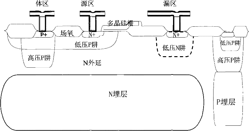
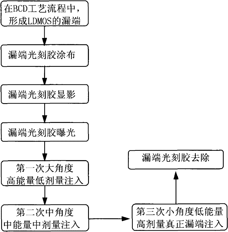
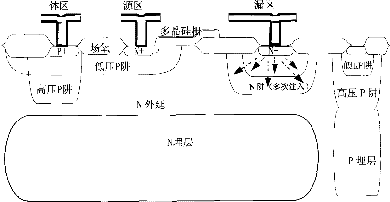
[0015] An embodiment of the LDMOS manufacturing method of the present invention is as follows figure 2 , image 3 As shown, its specific technological process is as follows:

[0016] 1. In the BCD process flow, the drain terminal of LDMOS is formed;

[0017] 2. Carry out photoresist coating at the drain end, develop the drain end, and expose the drain end, and perform more than two ion implantations on the drain end. The angle between the implantation direction and the wafer axis is from large to small, for example, from 45 degrees to 15 degrees, The energy of implanted ions is from high to low, for example, from 1500 kV to 70 kV, and the dose of implanted ions is from low to high, for example, from 1E14 to 1E16. Phosphorus ions, arsenic ions and antimony ions are implanted into the drain of the N-type lateral double-diffused MOS, and boron ions and boron-fluorine ions are implanted into the drain of the P-type lateral double-diffused MOS.

[0018] A preferred embodiment s...


PUM


Abstract

The invention discloses an LDMOS (Lateral Diffused Metal Oxide Semiconductor) manufacturing method, comprising the steps of: forming an LDMOS drain end in a BCD (Bipolar CMOS DMOS) process flow, and then carrying out ion implantation on the drain end for more than two times, wherein the angle between the direction of the ion implantation and a wafer axis gradually decreases, the energy of implanted ions gradually decreases and the dose of the implanted ions gradually increases. The LDMOS device manufactured by adopting the method has high working voltage, stable breakdown voltage and low cost.

Description

technical field [0001] The invention relates to a semiconductor process, in particular to an LDMOS manufacturing method. Background technique [0002] LDMOS (Lateral Diffused Medal-Oxide-Semiconductor, Lateral Diffused Medal-Oxide-Semiconductor) has relatively high operating voltage requirements. The operating voltage of the device is generally dependent on the carrier concentration and uniformity of the junction below the drain. In order to obtain a high working voltage of LDMOS, in the current BCD process platform, low-concentration doping is usually carried out under the drain of LDMOS, and then a long-term high-temperature push well is carried out to achieve a longer drift region. When the working voltage is increased, the depletion region Extend to the region with low doping concentration at the drain end to obtain a higher working voltage. This process mainly uses low-voltage wells or high-voltage wells. It requires long-term annealing of high-temperature furnace tube...

Claims


Application Information

Patent Timeline
Patent Type & Authority Patents(China)
IPC IPC(8): H01L21/336H01L21/265
Inventor 王海军张帅
Owner SHANGHAI HUAHONG GRACE SEMICON MFG CORP
Features
  • R&D
  • Intellectual Property
  • Life Sciences
  • Materials
  • Tech Scout
  • Unparalleled Data Quality
  • Higher Quality Content
  • 60% Fewer Hallucinations
Learn More