Method and device for preparing cadmium selenide sulfide nano material with monotonous and continuous variable band gap

A technology of cadmium sulfur selenide and nanomaterials, which is applied in the direction of nanotechnology, nanotechnology, nanostructure manufacturing, etc., can solve the problems of limited application, difficulty in achieving continuous adjustment and continuous wide spectrum, and achieve wide application range and preparation Simple method and low cost effect

Inactive Publication Date: 2011-01-12
ZHEJIANG UNIV
View PDF2 Cites 16 Cited by
  • Summary
  • Abstract
  • Description
  • Claims
  • Application Information

AI Technical Summary

Problems solved by technology

This method can obtain all spectra of fluorescence from ultraviolet to red, but each spectrum can only be used on one material, which limits its application, and it is difficult to achieve truly continuously adjustable and continuous wide spectrum on the device

Method used


Image

  • Method and device for preparing cadmium selenide sulfide nano material with monotonous and continuous variable band gap
  • Method and device for preparing cadmium selenide sulfide nano material with monotonous and continuous variable band gap
  • Method and device for preparing cadmium selenide sulfide nano material with monotonous and continuous variable band gap

Examples


Embodiment 1

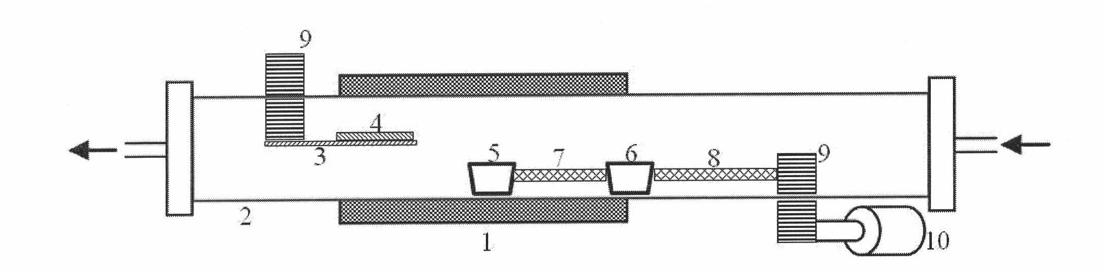
[0030] Embodiment 1 is the method for preparing the cadmium sulfide selenide nanoribbon that bandgap changes monotonously continuously, and the steps of this method are as follows:

[0031] 1. The experimental equipment is a tube-type high-temperature furnace 1 heated by resistance wire. Prepare a silicon chip 4 with a gold-plated thickness of 10 nm and place it on the quartz chip 3. The quartz chip is placed in the cooling zone of the high-temperature furnace. The bottom of the quartz chip can be just Accommodate the quartz boat 5, 0.5g of cadmium sulfide and cadmium selenide materials are placed in the quartz boat, the cadmium sulfide quartz boat 5 is placed in the middle of the tube-type high-temperature furnace, that is, the area with the highest temperature, and the cadmium selenide quartz boat 6 is placed in the tube Type high-temperature furnace 1 outside is close to the low-temperature zone of nitrogen inlet, a section of quartz rod 7 is placed between the two boats, an...

Embodiment 2

[0036] Embodiment 2 is a method for preparing cadmium sulfide selenide nanowires with monotonous and continuous band gap changes. The steps of the method are as follows:

[0037] The difference between the steps of this method and the steps of preparing nanobelts is that the growth temperature is 850° C., and other steps and parameters are the same as in Example 1.

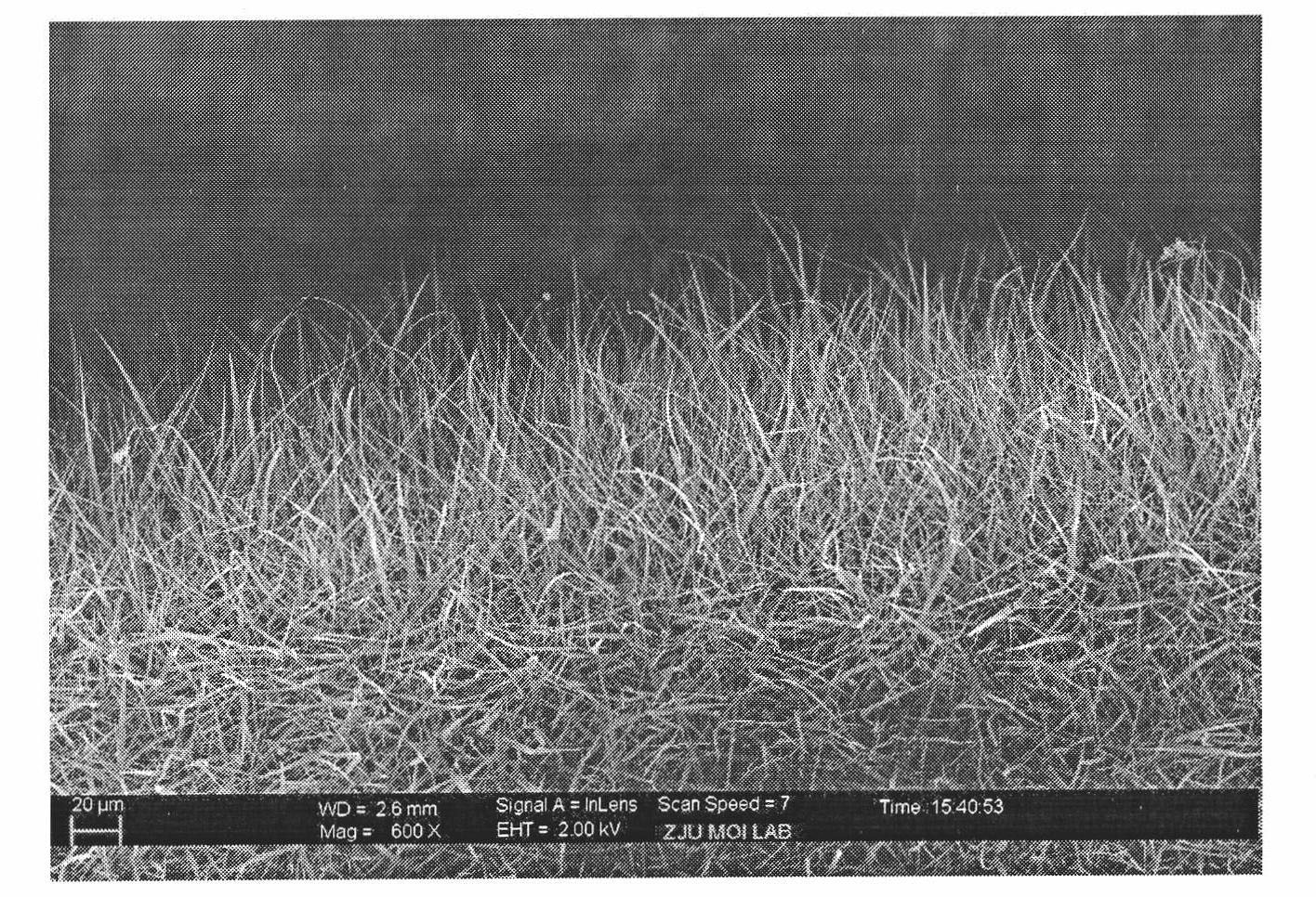
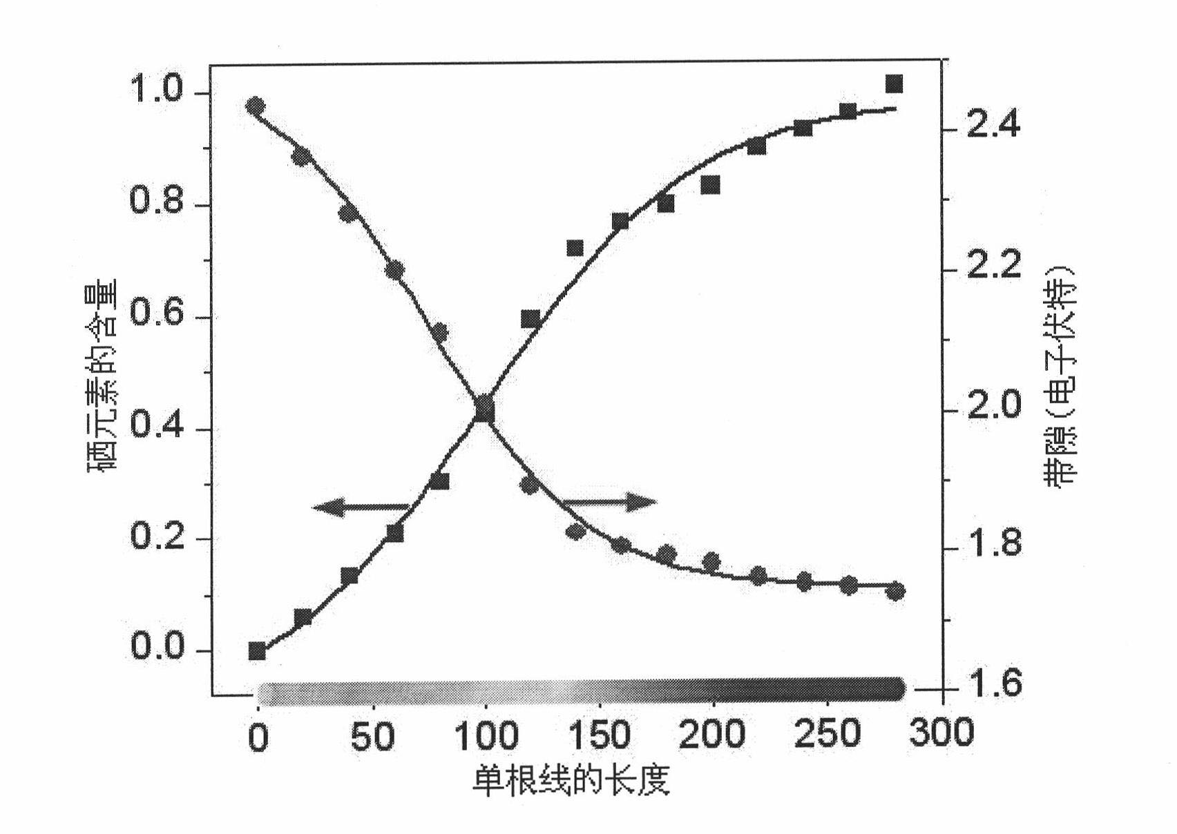
[0038] The length of the nanomaterial prepared in the above embodiment is on the order of hundreds of microns, the diameter of the nanowire is from 200nm to 2μm, the width of the nanoribbon is from 200nm to 5μm, and the thickness is less than 100nm. Depend on image 3 It can be seen that along a single nanoribbon, the content of selenium element and the band gap change monotonously and continuously, and the corresponding band gap of selenium element from 0 to 100% is 2.4ev to 1.7ev. Depend on Figure 4 It can be seen that the prepared nanoribbons are single crystals with good crystallinity, growing along the 001...


PUM

PropertyMeasurementUnit
thicknessaaaaaaaaaa
diameteraaaaaaaaaa
widthaaaaaaaaaa

Abstract

The invention discloses a method and a device for preparing a cadmium selenide sulfide nano material with monotonous and continuous variable band gap. According to the preparation method, based on a vapor deposition method, the positions of a cadmium sulfide quartz boat and a cadmium selenide quartz boat in a tubular high-temperature furnace are adjusted through a magnet to continuously adjust the vapor concentration ratio of cadmium sulfide to cadmium selenide during growing the nano material so as to realize monotonous continuous transition of the band gap on the same nano band or nano wire. The preparation method is simple and low in cost; the ratio of sulfur element to selenium element on the prepared single nano material can be continuously transited to 0: 1 from 1: 0; and the nano material has potential application value in the fields of tunable lasers, wideband lasers, white light LEDs, wide spectrum detectors and the like.

Description

technical field [0001] The invention relates to a method and a device for a cadmium sulfide selenide nanometer material, in particular to a method and a device for preparing a cadmium sulfide selenide nanometer material with monotonously and continuously changing band gaps. Background technique [0002] Semiconductor nanomaterials, including nanowires and nanoribbons, have been widely used in sensing, lasers, waveguides, optoelectronic devices and other fields due to their excellent physical properties, and have received extensive attention. As an important parameter of semiconductor materials, band gap directly determines the absorption and emission spectra of materials. Group II-IV compounds are a kind of adjustable wide bandgap semiconductor materials. For example, cadmium sulfur selenide can adjust the bandgap by changing the ratio of the two elements of sulfur and selenium, so as to obtain a single semiconductor material and a binary compound that cannot be achieved. b...

Claims


Application Information

Patent Timeline
Patent Type & Authority Applications(China)
IPC IPC(8): C01B19/04B82B3/00
Inventor 杨宗银谷付星童利民
Owner ZHEJIANG UNIV
Why Eureka
Try Eureka