VCO tuning curve compensation method and module thereof

A tuning curve, circuit module technology, applied in electrical components, power oscillators, multi-terminal-to-network, etc., can solve the problems of poor VCO phase noise performance, poor phase noise performance, high power consumption, etc., to simplify the implementation process, The effect of large tuning range and improved stability

Active Publication Date: 2011-01-12
杭州中科微电子有限公司
View PDF0 Cites 23 Cited by
  • Summary
  • Abstract
  • Description
  • Claims
  • Application Information

AI Technical Summary

Problems solved by technology

Although the VCO with this structure can be tuned in a large frequency range, it has major defects: First, the gain KVCO of the VCO varies greatly in the entire tuning range, and KVCO is large, and KVCO is very small in the low frequency band, which will seriously affect the stability of the entire frequency synthesizer; secondly, when there are many fixed capacitors, the MOS switch will make the resonant circuit, etc. The Q value of the effective capacitor decreases, especially in the low frequency band, which will not only lead to poor phase noise performance of the VCO, but also consume a lot of power
[0004]Compared with PN junction capacitors, traditional AMOS capaci...

Method used


Image

  • VCO tuning curve compensation method and module thereof
  • VCO tuning curve compensation method and module thereof
  • VCO tuning curve compensation method and module thereof

Examples


no. 1 Embodiment

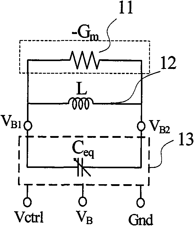
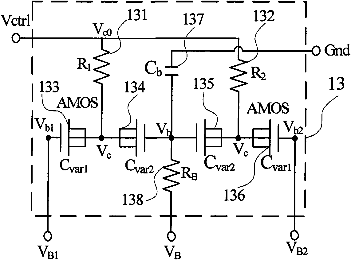
[0054] Figure 3a It is a functional block diagram of the tuning curve compensation VCO in the first embodiment. The VCO structure is an NMOS and PMOS complementary VCO with a tail current source, and a bias voltage V is added to the gate of the tail current source 37. B . The PMOS transistors 35 and 36 form a cross-coupled negative resistance amplifier, while the NMOS transistors 33 and 34 are cross-coupled to form another negative resistance amplifier. The two form a complementary NMOS and PMOS negative resistance amplifier with a tail current source. The variable capacitor 32 is electrically connected in parallel with the on-chip inductance 31 and the NMOS and PMOS complementary negative resistance amplifiers with a tail current source, Figure 3b for Figure 3a The tuning curve compensation VCO block diagram of the first embodiment is an electrical schematic diagram of the AMOS capacitor network for tuning curve compensation of the variable capacitor 32 . The equivalen...

no. 2 Embodiment

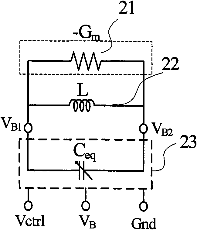
[0056] Figure 4a It is a schematic block diagram of the tuning curve compensation VCO in the second embodiment, and the PMOS transistor 43 is applied with a bias voltage V on the gate. B tail current source. PMOS transistors 44 and 45 constitute a cross-coupled negative resistance amplifier. The VCO structure is a PMOS negative resistance amplifier type VCO with tail current, an on-chip symmetrical inductor 41 with a center tap and a PMOS negative resistance amplifier with a tail current source, and the variable capacitor 42 is electrically connected in parallel. The variable capacitor 42 is composed of a capacitance network that adopts tuning curve compensation, and its specific schematic diagram is as follows Figure 4b As shown in the dashed box, the tuning curve compensation method adopted by the equivalent capacitance is the positive frequency characteristic compensation method shown in Figure 1, Figure 4b 431-438 are the same as 131-138 in Fig. 1 respectively. Simi...

no. 3 Embodiment

[0058] Figure 5a It is a functional block diagram of the tuning curve compensation VCO in the third embodiment. The VCO structure is an NMOS negative resistance amplifier type VCO with tail current. NMOS transistor 55 applies a bias voltage V to the grid B The drain of the tail current source is connected to the center tap of the on-chip symmetrical inductor 51 . NMOS transistors 53 and 54 constitute a cross-coupled negative resistance amplifier. An on-chip symmetrical inductor 51 with a center tap and an NMOS cross-coupled negative resistance amplifier are electrically connected in parallel with the variable capacitor 52, and the parallel connection port is V B1 and V B2 . The variable capacitor 52 is composed of a capacitor network that uses tuning curve compensation. The specific schematic diagram of the equivalent capacitor 52 is shown in the dotted line box, and the tuning curve compensation method adopted by the equivalent capacitor is the positive frequency chara...


PUM


Abstract

The invention provides a VCO tuning curve compensation method. In the method, a negative resistance amplifier and an inductor are connected with both ends of a variable capacitor to form a parallel-connection structure, wherein the variable capacitor structure is a five-end AMOS capacitance network, and one end is a tuning curve compensation control end of the AMOS capacitance network, which changes the equivalent capacitance of the AMOS capacitance network by adjusting the DC voltage of a control end to obtain an approximate linearized change curve with respect to VCO output frequency and VCO control voltage, thereby realizing the VCO tuning curve compensation, improving the VCO stability and enabling a VCO circuit module to work in the area having a higher Q value. The invention also provides a VCO circuit module of a differential circuit structure formed by the method. The AMOS capacitance network comprises four AMOS varactors and one RC low-pass filter, wherein the four AMOS varactors are connected in series two by two and are symmetrically arranged, and the specific arrangement mode includes grid electrode series connection and substrate series connection. The VCO module performs voltage control on the AMOS varactors to change the oscillator frequency, and realizes the tuning curve compensation to enable the frequency tuning curve to be approximately linearized by changing the DC voltage of the compensation control end of the tuning curve, thereby realizing a larger frequency tuning range.

Description

technical field [0001] The invention relates to the technical field of wireless communication electronic circuits, relates to a voltage-controlled oscillator VCO, in particular to a tuning curve compensation VCO method and a module thereof. Background technique [0002] In the mobile handheld wireless transceiver terminal, the voltage-controlled oscillator VCO is one of the most critical modules. The phase noise performance of the VCO directly affects the receiving sensitivity and blocking performance of the transceiver. With the development of wireless communication technology, a single chip in a communication system is required to be compatible with many different frequency bands and modes. Therefore, as a multi-band and multi-mode transceiver, its voltage-controlled oscillator VCO is required to cover a certain frequency range, so the research and development of wideband VCO has become an important topic for wireless communication electronic circuits. [0003] There are ...

Claims


Application Information

Patent Timeline
IPC IPC(8): H03B7/00H03H11/02
Inventor 肖时茂马成炎叶甜春
Owner 杭州中科微电子有限公司
Why Eureka
Try Eureka