Manufacturing method of GaInP/GaAs/InGaAsP/InGaAs four-junction solar battery

A technology of solar cells and manufacturing methods, applied in the field of solar photovoltaics, can solve problems such as increasing battery manufacturing costs, increasing battery efficiency factors, and increasing battery process difficulties, so as to improve photoelectric conversion efficiency, eliminate factors affecting device performance, and reduce The effect of small heat loss

Inactive Publication Date: 2011-01-19
SUZHOU INST OF NANO TECH & NANO BIONICS CHINESE ACEDEMY OF SCI
2 Cites 40 Cited by

AI-Extracted Technical Summary

Problems solved by technology

Therefore, it is necessary to obtain a thin layer of Ge before bonding, which will greatly increase the process difficulty of battery development.
In addition, the four-junction cell that matches the solar spectrum can also be obta...

Method used

[0021] As shown in Figure 1, the present invention is used in the GaInP/GaAs/solar cell and InGaAsP/InGaAs solar cell before and after bonding cell structure and bonding schematic diagram. It can be clearly seen from the accompanying drawings: the double-junction cell is grown on the GaAs substrate first with a GaAs cell, and then with a lattice-matched GaInP cell; with a lattice-matched InGaAs cell grown on an InP substrate, and then with a lattice matching InGaAsP cells. Since lattice matching is used for growth, the difficulty of material growth will not be increased due to lattice mismatch, and dislocations will not be generated due to stress release of the epitaxial layer, which will affect the quality of the crystal and thus affect the performance of the device; in addition, on GaAs substrates GaAs tunneling junctions are grown on the top of the GaInP battery on the InP substrate, and an InP tunneling junction is grown on the top of the InGaAsP battery on the InP substrate to reduce the resistance at the bonding interface and avoid a large voltage drop at the interface, which affects bat...

Abstract

The invention discloses a manufacturing method of a GaInP/GaAs/InGaAsP/InGaAs four-junction solar battery. By utilizing a wafer bonding method, the GaInP/GaAs/InGaAsP/InGaAs four-junction solar battery is integrated by a GaInP/GaAs double-junction solar battery growing based on a GaAs substrate and a InGaAsP/InGaAs double-junction solar battery growing based on an InP substrate; by utilizing the InP as a supporting substrate, the four-junction solar battery with respective band gap energies of 1.9/1.4/1.05/0.72 eV is realized, sunlight full spectral absorption and energy conversion are realized to a greater degree, and 32.8 percent of efficiency is realized in irradiation of AM1.5G and under the sun. Based on the development of two kinds of double-junction batteries, the bonded four-junction solar battery reduces the shortages of high cost caused by utilizing a plurality of different substrates in a mechanical cascade solar battery system and complex optical system and optical loss in an optical integrated battery, and effectively solves the problem of lattice mismatching of growing a uniwafer four-junction cascade semiconductor solar battery material. The high voltage and low current outputs are realized and the resistance consumption in a high concentrator battery is reduced.

Application Domain

Technology Topic

Band gapCell material +11

Image

  • Manufacturing method of GaInP/GaAs/InGaAsP/InGaAs four-junction solar battery
  • Manufacturing method of GaInP/GaAs/InGaAsP/InGaAs four-junction solar battery

Examples

  • Experimental program(1)

Example Embodiment

[0019] In order to make the above objectives, features and advantages of the present invention more obvious and easy to understand, the following is specifically described in detail in conjunction with specific embodiments of the present invention as follows:
[0020] 1) Cell growth before bonding
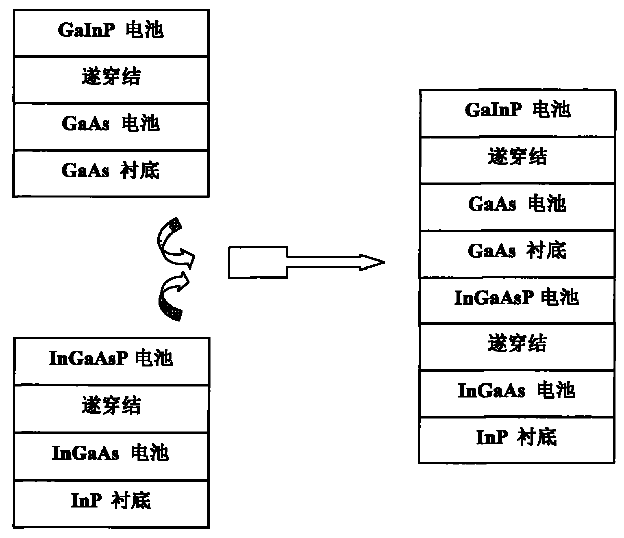
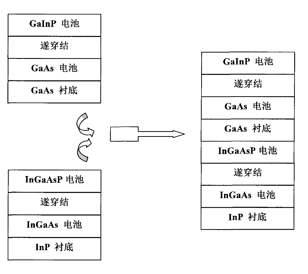
[0021] As shown in FIG. 1, it is a schematic diagram of the battery structure before and after the bonding of the GaInP/GaAs/solar cell and the InGaAsP/InGaAs solar cell used in the present invention. It can be clearly seen from the figure that the double-junction battery first grows GaAs battery on GaAs substrate, and then grows lattice-matched GaInP battery; grows lattice-matched InGaAs battery on InP substrate, and then grows lattice Matched InGaAsP battery. Because they are all grown by lattice matching, it will not increase the difficulty of material growth due to lattice mismatch, and will not cause dislocations due to the stress release of the epitaxial layer, which will affect the crystal quality and further affect the device performance; in addition, on the GaAs substrate The GaAs tunnel junction is grown on the top of the GaInP battery, and the InP tunnel junction is grown on the top of the InGaAsP battery on the InP substrate to reduce the resistance at the bonding interface and avoid a large voltage drop at the interface, which affects battery performance.
[0022] 2) Bonding of wafers
[0023] In the present invention, the bonding interface is p+GaAs/n+InP, where the thinned GaAs substrate serves as the back surface layer of the battery, and InP is the top structure of the InGaAsP battery. GaAs needs to choose a doping concentration higher than 1.0×10 19 P-type substrate, the substrate needs to be thinned to 10-30nm; the doping concentration of n+InP on the top layer needs to be higher than 1.0×10 19 , Thickness range: 15-30nm. Then perform bonding and annealing to form a good contact and reduce the influence of the interface resistance, thereby obtaining an ideal bonding interface with a small interface resistance; the annealing temperature is 400-550℃, which is much lower than the material growth temperature and will not affect To the quality of materials and device performance. After that, the battery preparation is completed according to the standard battery process, including a series of output power, size and shape, and packaging process steps suitable for installation, to obtain a four-junction solar cell as shown on the right side of Figure 1.
[0024] To sum up, it is a detailed description of a specific embodiment of the present invention, and does not constitute any limitation to the scope of protection of this case. All technical methods formed by equivalent transformations or equivalent substitutions fall within the protection scope of the present invention.

PUM

no PUM

Description & Claims & Application Information

We can also present the details of the Description, Claims and Application information to help users get a comprehensive understanding of the technical details of the patent, such as background art, summary of invention, brief description of drawings, description of embodiments, and other original content. On the other hand, users can also determine the specific scope of protection of the technology through the list of claims; as well as understand the changes in the life cycle of the technology with the presentation of the patent timeline. Login to view more.

Similar technology patents

Ion source

InactiveUS20060284104A1Reduce heat lossEnhance heating efficiencyElectric arc lampsMaterial analysis by optical meansEngineeringIon source
Owner:NISSIN ION EQUIP CO LTD

Electric grill

InactiveUS20050205544A1Reduce heat lossDomestic stoves or rangesElectrical heating fuelElectric heatingElectricity
Owner:THE OUTDOOR GREATROOM LLLP

Classification and recommendation of technical efficacy words

  • Reduce heat loss
  • Achieve absorption

Bag-in-box beverage container

InactiveUS20060097005A1Reduce heat lossFlexible containersPliable tubular containersCorrugated fiberboardEngineering
Owner:WESTROCK SHARED SERVICES LLC

System for sensing particulate matter

InactiveUS20150355066A1Reduce heat lossUniform depositionInternal-combustion engine testingExhaust apparatusEngineeringParticulate matter sampler
Owner:FORD GLOBAL TECH LLC

Compact steam reformer

Owner:WS REFORMER

Light splitting manufacturing process for five-junction solar cell system

Owner:SUZHOU INST OF NANO TECH & NANO BIONICS CHINESE ACEDEMY OF SCI
Why Eureka
Try Eureka