Sheet structure, semiconductor device and method of growing carbon structure
A growth method and structure technology, applied in the direction of semiconductor devices, semiconductor/solid-state device manufacturing, semiconductor/solid-state device components, etc., can solve the problems of reliability deterioration, improve thermal conductivity and electrical conductivity, prevent manufacturing costs, Effect of preventing increase of manufacturing cost
- Summary
- Abstract
- Description
- Claims
- Application Information
AI Technical Summary
Problems solved by technology
Method used
Image

Examples
no. 1 approach
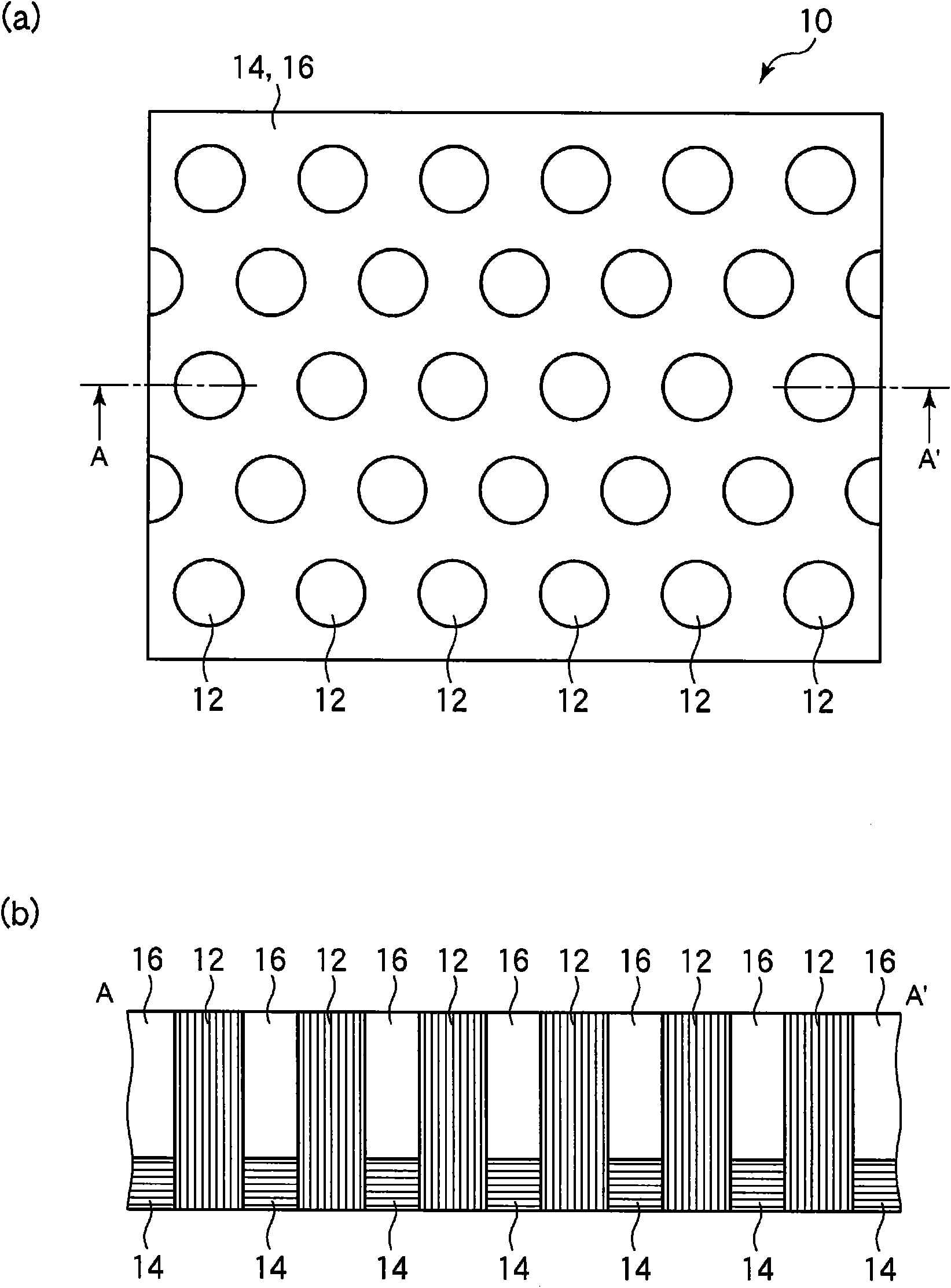
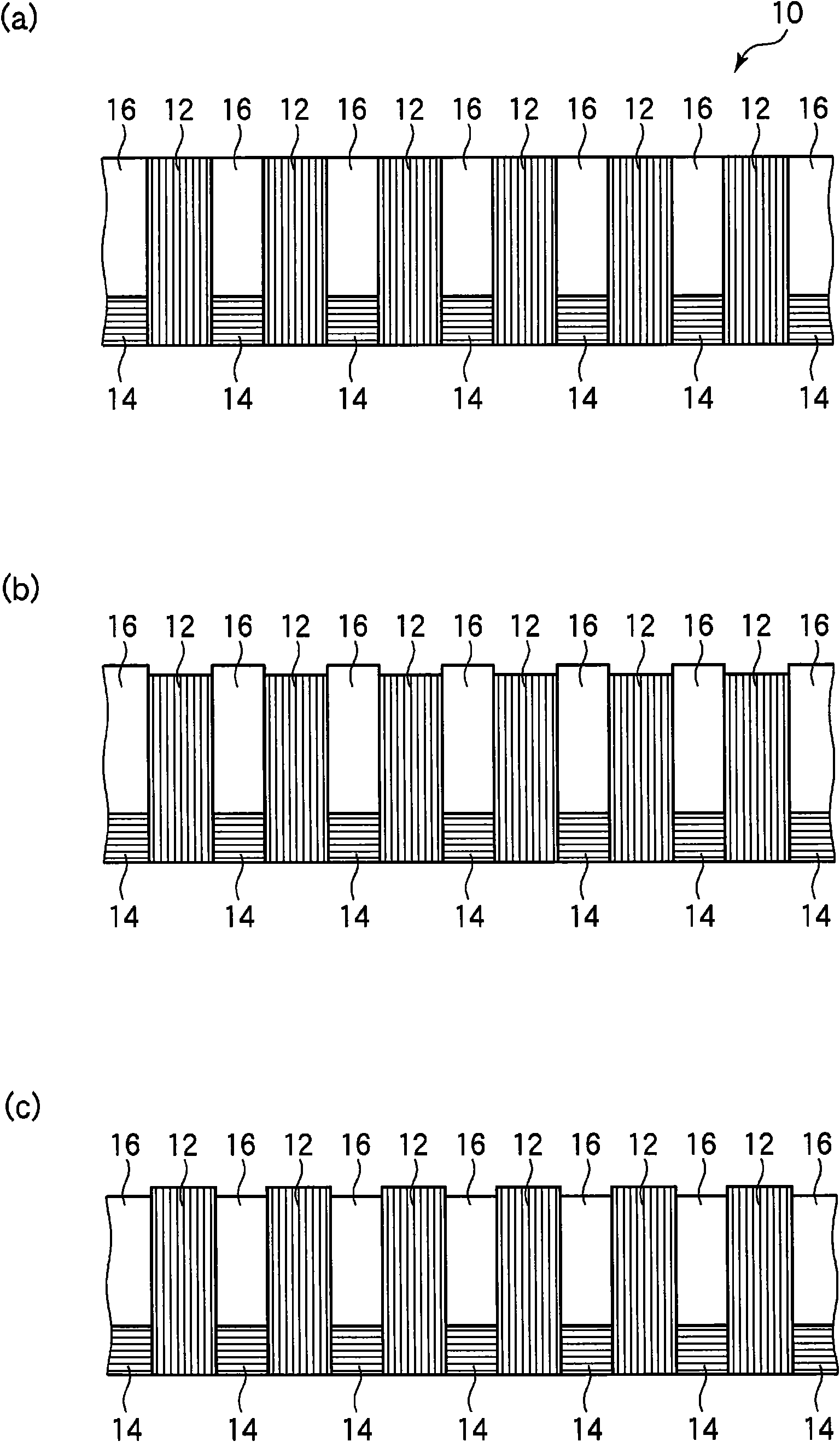
[0079] use Figure 1 to Figure 5 The carbon nanotube sheet and its manufacturing method according to the first embodiment of the present invention will be described.
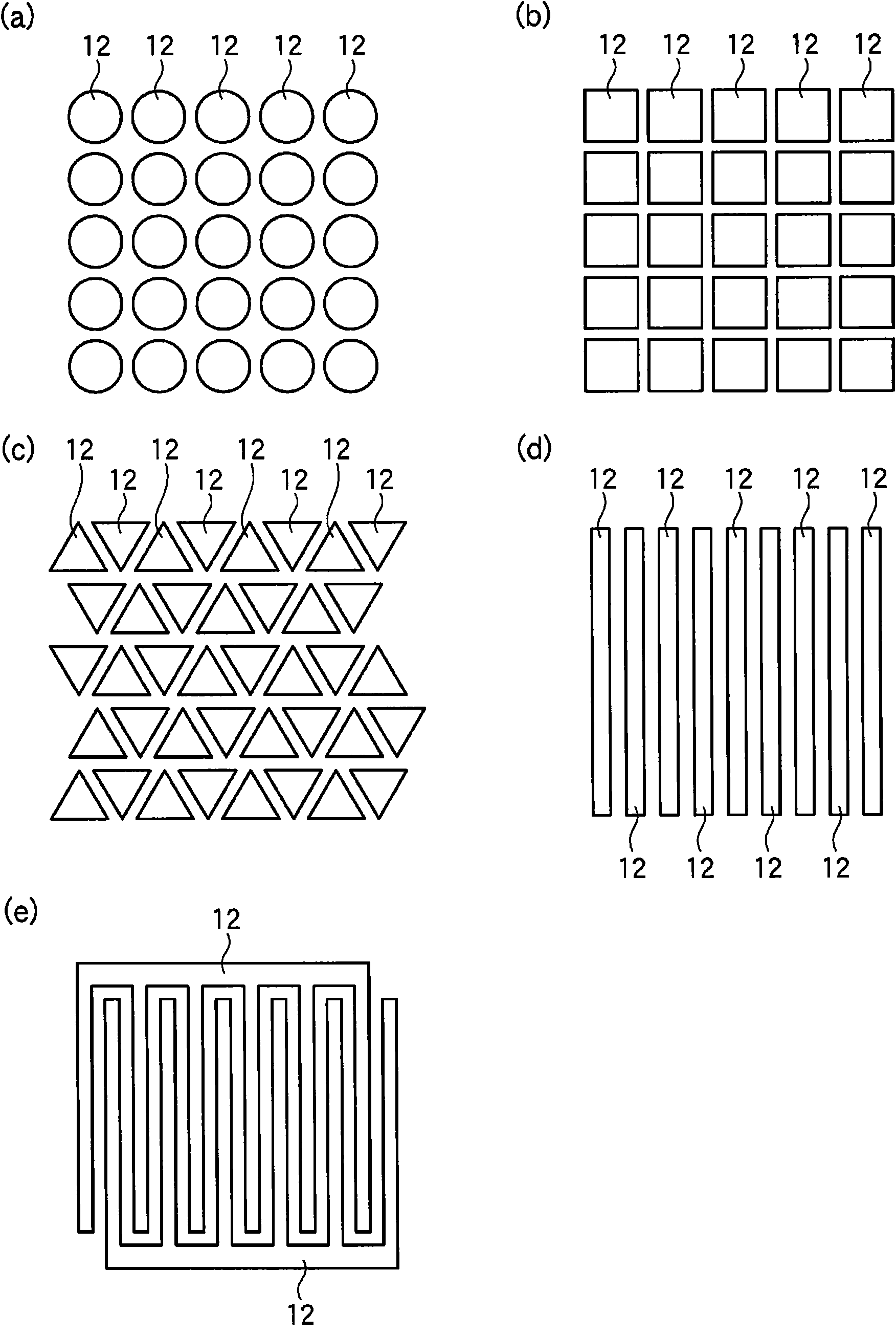
[0080] figure 1 It is a plan view and a schematic cross-sectional view showing the structure of a carbon nanotube sheet according to the present embodiment, figure 2 is a plan view showing the shape of the carbon nanotube bundles of the carbon nanotube sheet according to the present embodiment, image 3 is a schematic cross-sectional view showing the structure of a carbon nanotube sheet according to this embodiment, Figure 4 and Figure 5 It is a cross-sectional view showing the steps of the method for producing the carbon nanotube sheet according to the present embodiment.
[0081] First, use figure 1 The structure of the carbon nanotube sheet according to this embodiment will be described. figure 1 (a) and figure 1 (b) is a plan view and a cross-sectional view showing the structure of the carbon nanot...
no. 2 approach
[0143] use Figure 6 to Figure 9 The carbon nanotube sheet and its manufacturing method according to the second embodiment of the present invention will be described. right with Figure 1 to Figure 5 In the carbon nanotube sheet and its production method according to the first embodiment shown, the same components are given the same reference numerals, so descriptions or brief descriptions are omitted.
[0144] Figure 6 It is a plan view and a schematic cross-sectional view showing the structure of a carbon nanotube sheet according to the present embodiment, Figure 7 is a schematic cross-sectional view showing the structure of a carbon nanotube sheet according to a modified example of the present embodiment, Figure 8 and Figure 9 It is a cross-sectional view showing the steps of the method for producing the carbon nanotube sheet according to the present embodiment.
[0145] First, use Figure 6 The structure of the carbon nanotube sheet according to this embodiment w...
no. 3 approach
[0192] use Figure 10 to Figure 13 A semiconductor device and a manufacturing method thereof according to a third embodiment of the present invention will be described.
[0193] Figure 10 is a schematic cross-sectional view showing the structure of the semiconductor device according to the present embodiment, Figure 11 to Figure 13 It is a cross-sectional view showing the steps of the manufacturing method of the semiconductor device according to the present embodiment.
[0194] First, use Figure 10 The structure of the semiconductor device according to this embodiment will be described.
[0195] A wiring layer 42 is formed on the substrate 40 . On a region of the substrate 40 other than the region where the wiring layer 42 is formed, an interlayer insulating film 44 is formed. On one end of the wiring layer 42 , a via wiring 64 made of carbon nanotube bundles is formed via the TiN film 52 . A wiring layer 66 made of graphite and connected to the via wiring 64 is forme...
PUM
| Property | Measurement | Unit |
|---|---|---|
| thickness | aaaaa | aaaaa |
| thickness | aaaaa | aaaaa |
| thickness | aaaaa | aaaaa |
Abstract
Description
Claims
Application Information