Radiation imaging system based on photoluminescence image plate with radiation memory function
A technology of radiation imaging and photoluminescence, which is applied in the field of radiation measurement, can solve problems such as the inability to detect weak radiation signals, and achieve the effect of improving the signal-to-noise ratio
- Summary
- Abstract
- Description
- Claims
- Application Information
AI Technical Summary
Problems solved by technology
Method used
Image
Examples
Embodiment 1
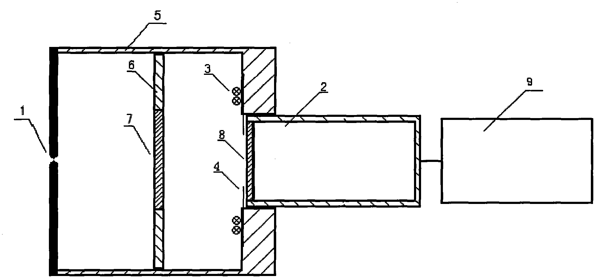
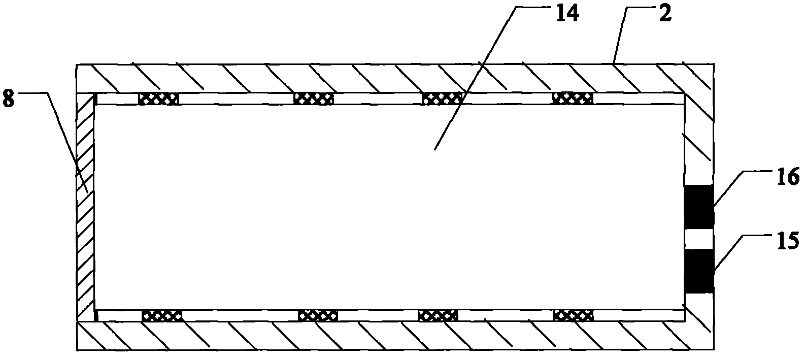
[0030] The radiation imaging system based on the photoluminescent image plate with radiation memory function provided by this embodiment, such as figure 1 As shown, it includes a light-shielding frame 5, a pinhole collimator 1, a position-sensitive light detection module 2, a control and image processing module 9, and the like. The pinhole collimator 1 is located at the front end of the shading frame 5, the position-sensitive photodetection module 2 is placed at the rear end of the shading frame 5 and its light detection surface is facing the pinhole collimator 1, and the control and image processing module 9 is connected to the pinhole collimator 1. The position-sensitive photodetection module 2 is connected, and the key is that an image plate 7 made of a photoluminescent material with radiation memory function is also placed between the pinhole collimator 1 and the position-sensitive photodetection module 2; An excitation light source 3 corresponding to the photoluminescent ...
Embodiment 2
[0043] Other technical solutions remain unchanged, and the difference from Embodiment 1 is:
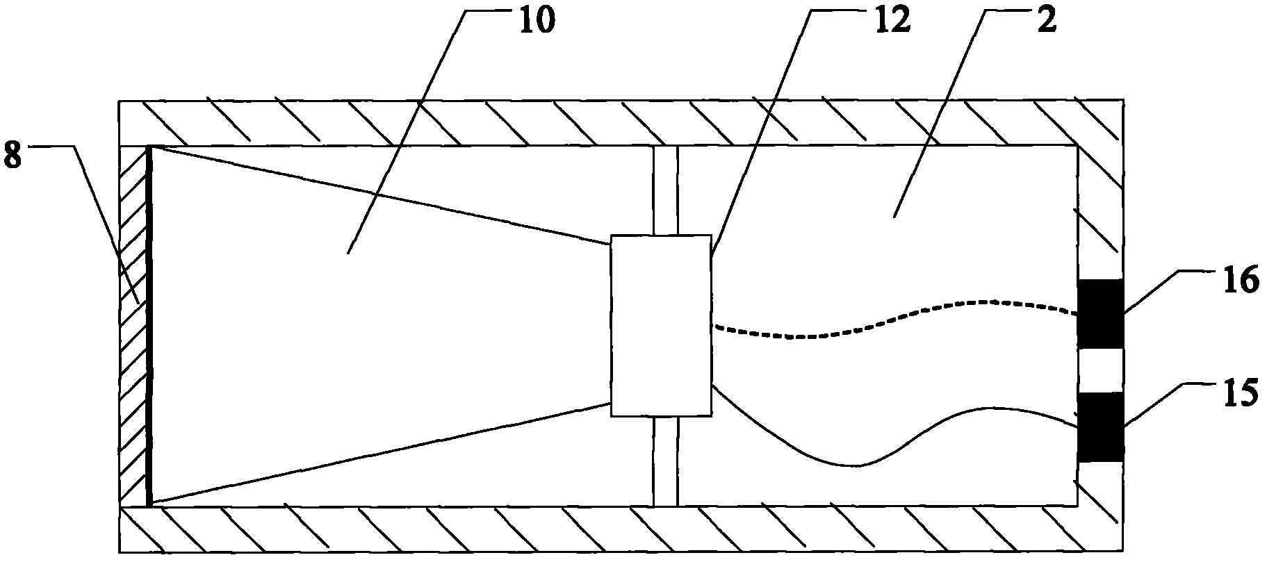
[0044] The photodetector adopted in the present embodiment is a charge-coupled device (CCD) or CMOS 12, and a tapered optical fiber imaging bundle 10 is placed between the optical filter 8 and the CCD / CMOS 12, such as image 3 shown. Fluorescent signals excited by the image plate 7 are coupled to the surface of the CCD / CMOS 12 through the tapered optical fiber imaging bundle 10 and measured, while retaining position information and intensity information.
Embodiment 3
[0046] Other technical solutions remain unchanged, and the difference from Embodiment 1 is:
[0047] The photodetector adopted in the present embodiment is a charge-coupled device (CCD) or CMOS 12, and an imaging lens group 13 is placed between the optical filter 8 and the CCD / CMOS 12, and the photosensitivity of the CCD / CMOS 12 The chip is located on the image plane of the imaging lens group 13, such as Figure 4 shown. The fluorescent signal excited by the image plate 7 is imaged to the surface of the CCD / CMOS 12 through the conical imaging lens group 13 and measured, while retaining position information and intensity information.
PUM
 Abstract
Description
Claims
Application Information


