

Method of dielectric film treatment
A technology of dielectric film and dielectric material, applied in circuits, electrical components, semiconductor/solid-state device manufacturing, etc., can solve problems such as metal passivation, electrical integrity impact, etc.
- Summary
- Abstract
- Description
- Claims
- Application Information
AI Technical Summary
Problems solved by technology
Method used
Image

Examples
Embodiment Construction
[0021] Some embodiments for better and more efficient cleaning of substrate surfaces will now be described. It will be apparent, however, to one skilled in the art, that the present invention may be practiced without some or all of these specific details. In other instances, well known process operations have not been described in detail in order not to unnecessarily obscure the present invention.
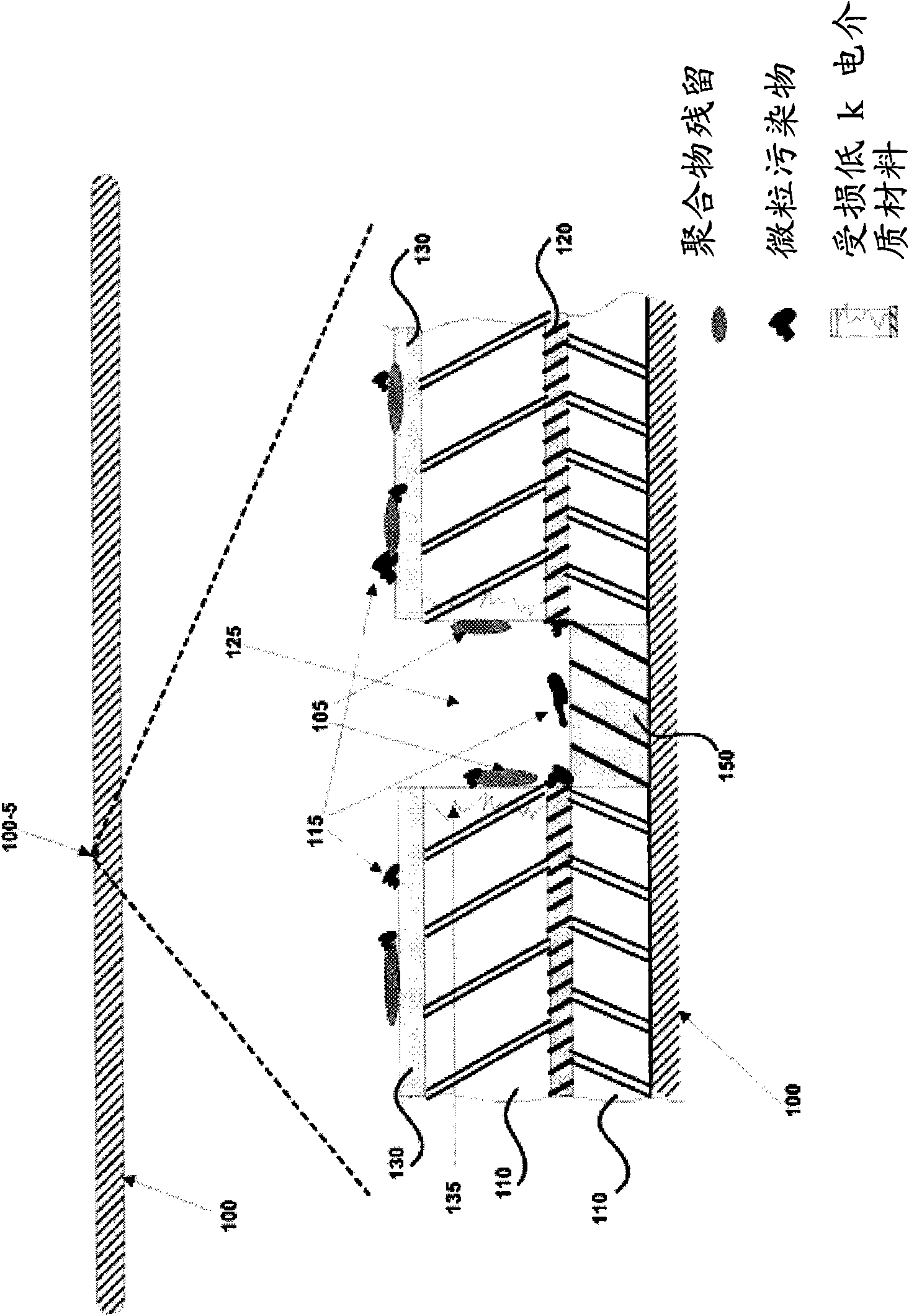
[0022] Traditional methods have focused primarily on providing solutions that remove specific types of contaminants from the substrate surface. It is well known in the industry that there is more than one type of contamination that can potentially cause damage to the substrate surface. figure 1A simplified schematic diagram of a damaged portion 100-5 of a substrate 100 with various contaminants is depicted. As shown, portion 100 - 5 of substrate 100 includes a low-k dielectric film layer 110 formed on substrate 100 . The low-k dielectric film layer 110 is formed using any one of...
PUM
 Abstract
Description
Claims
Application Information