High-resolution aspheric photoetching object lens

A lithography objective lens and high-resolution technology, applied in the field of high-resolution projection lithography objective lenses, can solve the problems of large total thickness and weight of the deep ultraviolet lithography objective lens, simplify the objective lens manufacturing process, improve the quality of the objective lens, and improve the imaging quality effect

Active Publication Date: 2011-02-16
BEIJING INSTITUTE OF TECHNOLOGYGY
View PDF9 Cites 3 Cited by
  • Summary
  • Abstract
  • Description
  • Claims
  • Application Information

AI Technical Summary

Problems solved by technology

[0005] In order to further improve the imaging quality and solve the problem that the total thickness and weight of the deep ultraviolet lithography objective lens in the prior art are relatively large, the present invention proposes a high-resolution aspheric lithography objective lens

Method used


Image

  • High-resolution aspheric photoetching object lens
  • High-resolution aspheric photoetching object lens
  • High-resolution aspheric photoetching object lens

Examples


Embodiment Construction

[0028] In order to better illustrate the purpose and advantages of the present invention, the present invention will be further described below in conjunction with the accompanying drawings and specific embodiments.

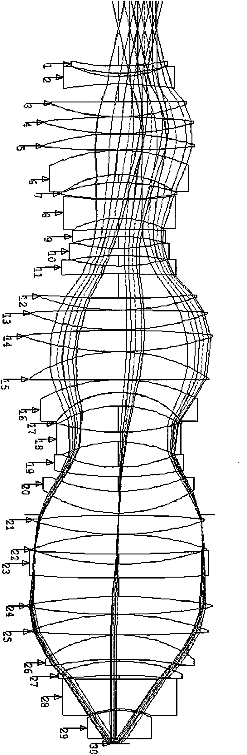
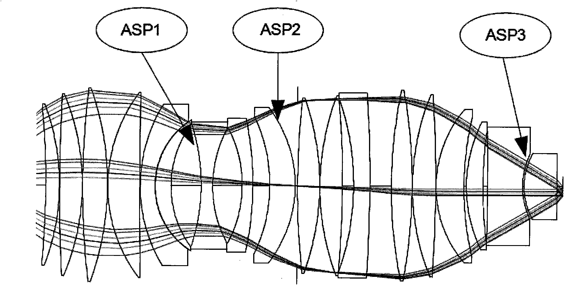
[0029] The high-resolution aspheric lithography objective lens of this embodiment is composed of front and rear lens groups, and a total of 29 spherical lenses are used, including three 10-degree aspheric surfaces. as attached figure 1 As shown, lenses 1 to 20 are the front lens group, lenses 21 to 29 are the rear lens group, and 30 is the image plane, that is, the surface where the silicon chip is located. The lens material uses fused silica (refractive index of 1.560326 at the system center wavelength of 193.368nm) as the main lens material, and calcium fluoride (refractive index of 1.501455 at the system center wavelength) as the material used to correct chromatic aberration.

[0030] The front lens group includes a first meniscus lens 1, a first negative len...


PUM

PropertyMeasurementUnit
refractive indexaaaaaaaaaa

Abstract

The invention relates to a high-resolution aspheric photoetching object lens which belongs to the technical field of a high-resolution projection photoetching object lens. The high-resolution aspheric photoetching object lens comprises a front lens set and a rear lens set. The numerical aperture is 0.75, and 29 lenses are used in total, 3 surfaces of the 29 lenses use aspheric surfaces for 10 times; and the lenses are made of fused quartz and calcium fluoride used for correcting chromatic aberration. The invention further improves the resolution of the existing projection photoetching object lens, and greatly improves the imaging quality by using a small quantity of low order aspheric surfaces; and the radius and the thickness space of each lens element are changed in the optimizing process to fit with the aspheric surface so as to carry out aberration correction better. When the central optical line is used as a reference, the wave aberration of homochromy mean square root is less than nm, and the aberrance is less than 0.7nm.

Description

technical field [0001] The invention relates to a high-resolution aspheric lithography objective lens, which belongs to the technical field of high-resolution projection lithography objective lens. Background technique [0002] Photolithography is an integrated circuit manufacturing technology that uses optical methods to transfer the circuit pattern on the mask plate to the silicon wafer. Almost all integrated circuits are manufactured using optical lithography. Initially, semiconductor devices were manufactured using contact lithography technology in which masks were attached to silicon wafers. In 1957, contact lithography technology realized the manufacture of DRAM (Dynamic Random Access Memory) with a feature size of 20 μm. After that, the semiconductor industry introduced proximity lithography technology with a certain gap between the mask and the silicon wafer, and DRAMs with feature sizes of 10 μm and 6 μm were manufactured in 1971 and 1974, respectively. In 1977, t...

Claims


Application Information

Patent Timeline
Patent Type & Authority Applications(China)
IPC IPC(8): G02B13/14G02B13/00G02B1/00G03F7/20G02B13/18G02B13/22
Inventor 李林马斌李艳秋刘丽辉韩星常军黄一帆
Owner BEIJING INSTITUTE OF TECHNOLOGYGY
Why Eureka
Try Eureka