Annealing process for reducing stress of silicon carbide crystals

An annealing process, silicon carbide technology, applied in crystal growth, chemical instruments and methods, post-processing details, etc., can solve problems such as crystal cracking

Active Publication Date: 2011-03-09
XINJIANG TANKEBLUE SEMICON +1
View PDF0 Cites 27 Cited by
  • Summary
  • Abstract
  • Description
  • Claims
  • Application Information

AI Technical Summary

Problems solved by technology

[0006] Aiming at the serious problem of crystal cracking caused by mechanical action in the process of getting silicon carbide crystals from the crucible lid and subsequent processing of the crystals, especially when the crystals are ground and rolled, the present invention mainly adopts secondary annealing (crystal growth) After the end, the in-situ annealing process in the furnace is the first annealing) to reduce the stress between the silicon carbide crystal and the crucible cover and inside the silicon carbide crystal, thereby eliminating the problem of crystal cracking caused by taking the crystal from the crucible cover and subsequent processing of the crystal, Improving SiC Crystal Yield

Method used


Image

  • Annealing process for reducing stress of silicon carbide crystals
  • Annealing process for reducing stress of silicon carbide crystals
  • Annealing process for reducing stress of silicon carbide crystals

Examples


Embodiment 1

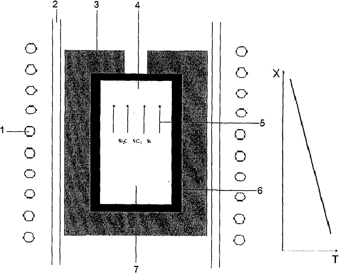
[0030] Put the 2-inch 6H semi-insulating silicon carbide crystal to be annealed directly into the annealing crucible together with the crucible cover, then add an appropriate amount of high-purity silicon carbide raw material around it, and place it in a graphite heating annealing furnace with good sealing performance. The furnace is 12 Hourly air leakage does not exceed 10 Pa. Design the insulation layer outside the crucible so that the temperature gradient is 15-20°C / cm when the crucible is at the annealing temperature. After installing the furnace, evacuate to 5 Pa and then fill with argon to 10,000 Pa. Turn on the power, heat up from 100°C to 2100°C at a speed of 200°C / h for 10 hours, keep the temperature for 10 hours, then cool down from 2100°C to 100°C at a speed of 200°C / h for 10 hours, and then turn off the power directly.

Embodiment 2

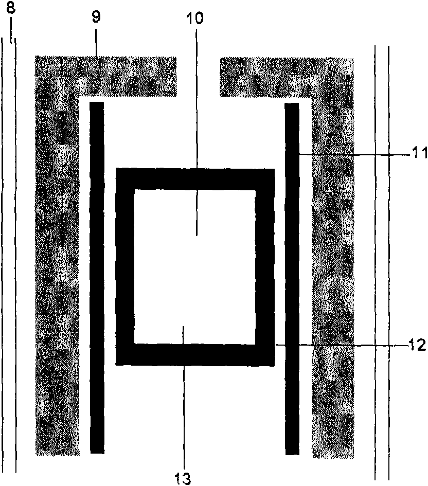
[0032] Put the 3-inch 4H conductive silicon carbide crystal to be annealed in the annealing crucible, then add an appropriate amount of conductive silicon carbide raw material around it, and then put it into a well-sealed induction coil heating annealing furnace, which will not leak for 12 hours more than 10 Pa. Design the insulation layer outside the crucible so that the temperature gradient is 10-15°C / cm when the crucible is at the annealing temperature. After installing the furnace, evacuate to 5 Pa and then fill with argon to 20,000 Pa. Turn on the power, raise the temperature from 100°C to 2100°C at a speed of 100°C / h for 20 hours, keep the temperature for 20 hours, then cool down from 2100°C to 100°C at a speed of 100°C / h for 20 hours, and then turn off the power directly.

Embodiment 3

[0034] Put the 4-inch 4H conductive silicon carbide crystal to be annealed in the annealing crucible, then add an appropriate amount of conductive silicon carbide raw materials around it, and then put it into a well-sealed induction coil heating annealing furnace, and the furnace will not leak more than 12 hours. 10 Pa. Design the insulation layer outside the crucible so that the temperature gradient is 5-10°C / cm when the crucible is at the annealing temperature. After installing the furnace, evacuate to 5 Pa and fill with argon to 40,000 Pa. Turn on the power, heat up from 100°C to 2100°C at a speed of 50°C / h for 40 hours, keep the temperature for 30 hours, then cool down from 2100°C to 100°C at a speed of 50°C / h for 40 hours, and then turn off the power directly.


PUM


Abstract

The invention is mainly applied in the retreatment field of the grown silicon carbide crystals. The annealing process specifically comprises the following steps: heating for 10-50 hours to an annealing temperature in an annealing furnace with good tightness and small temperature gradient (the temperature gradient of the surrounding of the crystals is 1-20 DEG C/cm) under the protection of an inert gas with the pressure of more than 10000Pa, keeping the temperature for 10-40 hours, and reducing the temperature for 10-50 hours, wherein the annealing temperature is 2100-2500 DEG C. Through the double annealing, the stress between the crystals and the crucible cover and the internal stress of the silicon carbide crystals are reduced, thus the breakage rate of the silicon carbide crystals is reduced in the subsequent processing step and the yield of the silicon carbide crystals is increased.

Description

technical field [0001] The present invention is mainly used in the field of post-processing of silicon carbide crystal growth, specifically, the secondary annealing process reduces the stress between the crystal and the crucible cover and the internal stress of the crystal to reduce the crystal damage rate in the subsequent processing process, thereby increasing the crystal yield . Background technique [0002] With the maturity of the development of the first-generation silicon semiconductor and the second-generation gallium arsenide semiconductor materials, their device applications are also reaching their limits. More and more fields of modern science and technology require materials with high frequency, high power, high temperature resistance, good chemical stability and can work in strong radiation environments. eV) has received great attention. These materials include II-VI, III-V, silicon carbide and diamond, etc., among which silicon carbide is the most mature techn...

Claims


Application Information

Patent Timeline
Patent Type & Authority Applications(China)
IPC IPC(8): C30B33/02
Inventor 彭同华汪波李龙远陈小龙刘春俊李河清朱丽娜吴星倪代秦王文军王刚王皖燕
Owner XINJIANG TANKEBLUE SEMICON
Why Eureka
Try Eureka