Method for manufacturing groove MOSFET (Metal-Oxide -Semiconductor Field Effect Transistor)

A kind of manufacturing method, technology of groove

Active Publication Date: 2012-12-12
FORCE MOS TECH CO LTD
View PDF1 Cites 0 Cited by
  • Summary
  • Abstract
  • Description
  • Claims
  • Application Information

AI Technical Summary

Problems solved by technology

When there is an applied voltage, the NPN bipolar transistor is easily turned on, which further deteriorates the avalanche breakdown characteristics of the device

Method used


Image

  • Method for manufacturing groove MOSFET (Metal-Oxide -Semiconductor Field Effect Transistor)
  • Method for manufacturing groove MOSFET (Metal-Oxide -Semiconductor Field Effect Transistor)
  • Method for manufacturing groove MOSFET (Metal-Oxide -Semiconductor Field Effect Transistor)

Examples


Embodiment Construction

[0065] The invention is explained in more detail below with reference to the accompanying drawings, in which preferred embodiments of the invention are shown. The invention can, however, be embodied in different ways and should not be limited to the embodiments described herein. For example, the description here refers more to N-channel trench MOSFETs, but clearly other devices are possible.

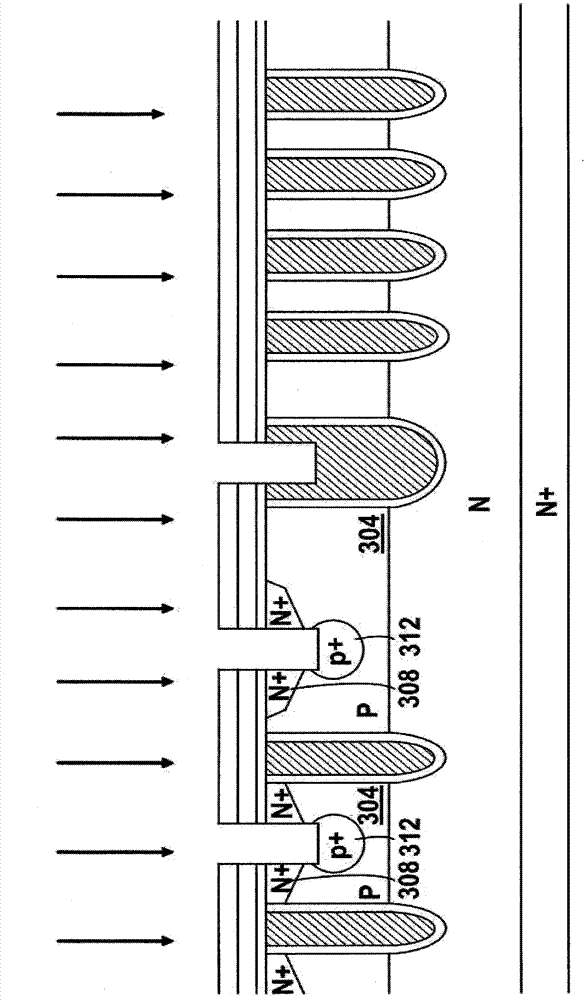
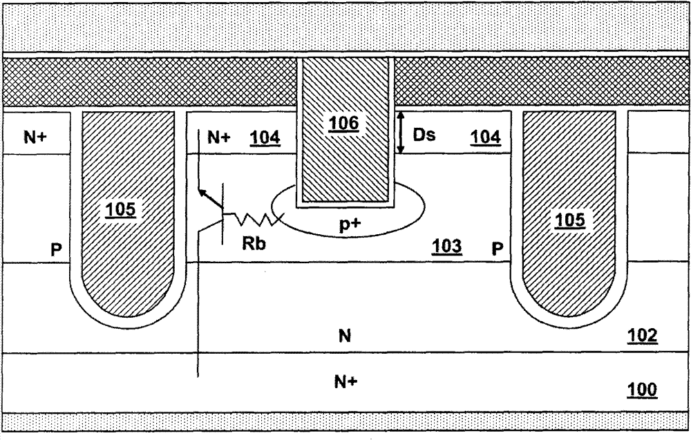
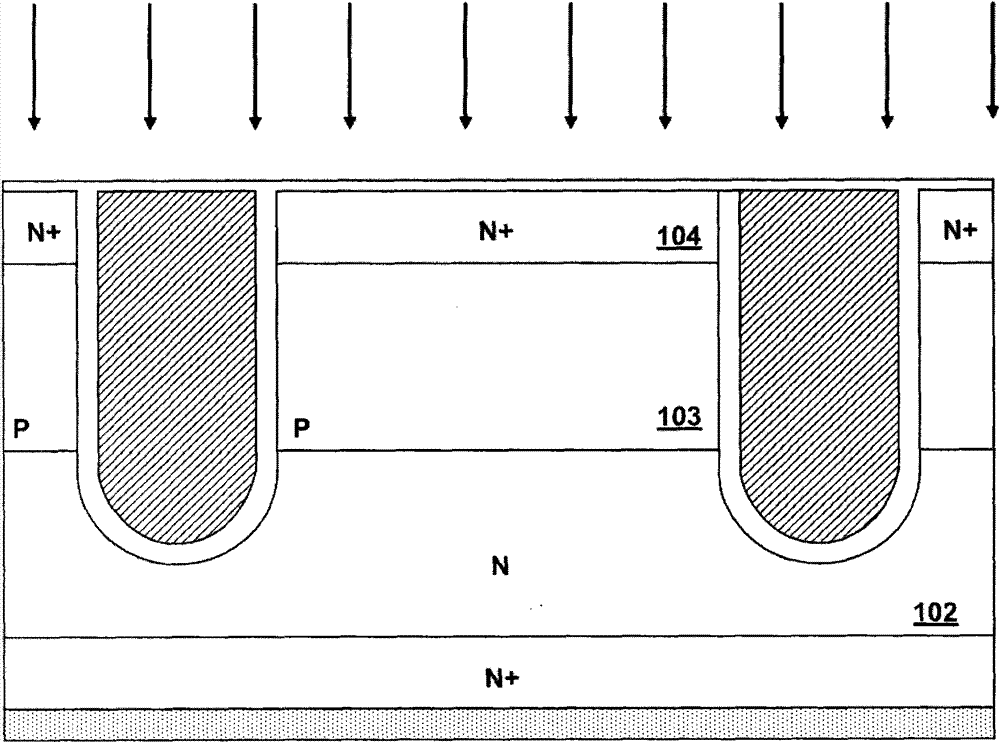
[0066] refer to Figure 3A A preferred embodiment of the invention is shown. The figure also shows Figure 2B or Figure 2C X of top view shown 1 -X 1 ’ sectional view. In the trench MOSFET according to this preferred embodiment, an N-type epitaxial layer 301 is formed on an N+ substrate 300, and a trench formed in the epitaxial layer is lined with a gate oxide 320 and filled with doped polysilicon Trench gates 311 are formed. The P-type body region 304 is formed in the epitaxial layer and is located between every two adjacent trench gates.

[0067] The N+ type source region 308 ...


PUM


Abstract

The invention discloses a groove MOSFET (Metal-Oxide -Semiconductor Field Effect Transistor) structure and a manufacturing method thereof. Different from the formation method of a groove MOSFET source region in the prior art, the source region of the groove MOSFET structure is formed by carrying out ion injection and diffusion of source-region majority carriers at an opening of a source body-contact groove so that the concentration distribution of the source-region majority carriers presents a Gaussian distribution along the surface direction of an epitaxial layer from the source body-contactgroove to a channel region, and the depth of the source region is gradually shallowed from the source body-contact groove to the channel region. A groove MOSFET device adopting the structure in the invention has the property of better avalanche breakdown than that of the prior art, and correspondingly, in the manufacturing process, the invention discloses a manufacturing method only needing to use a mask template for three times so that the production cost is greatly reduced.

Description

technical field [0001] The invention relates to a unit structure of a semiconductor power device, a device structure and a process manufacturing method. In particular, it relates to a trench MOSFET (Metal Oxide Semiconductor Field Effect Transistor) structure with improved avalanche breakdown characteristics and its manufacturing method using a three-layer mask. Background technique [0002] US Patent Publication No. US.6,888,196 discloses a trench MOSFET structure and manufacturing method, as shown in FIG. 1A . The structure of the trench MOSFET includes: a substrate 100 of N+ conductivity type; an epitaxial layer 102 of N conductivity type; a plurality of trench gates 105; a body region 103 of P conductivity type and a source region 104 of N+ conductivity type. Wherein, the source region 104 is formed by ion implantation and subsequent diffusion after being defined by a source region mask, as shown in FIG. 1B . Therefore, the source region 104 has the same doping concent...

Claims


Application Information

Patent Timeline
Patent Type & Authority Patents(China)
IPC IPC(8): H01L21/8234H01L21/336H01L27/088H01L29/78H01L29/36
Inventor 谢福渊
Owner FORCE MOS TECH CO LTD
Why Eureka
Try Eureka