[0018] The embodiments of the present invention will be described in detail below. This embodiment is implemented on the premise of the technical solution of the present invention. Detailed implementation modes and specific operation procedures are given, but the protection scope of the present invention is not limited to the following implementations. example.
[0019] In this example, the PCI bus is used as the computer bus example, and the IEEE 1394 bus is used as the field bus example, but the protection scope of the present invention is not limited to the described embodiments.
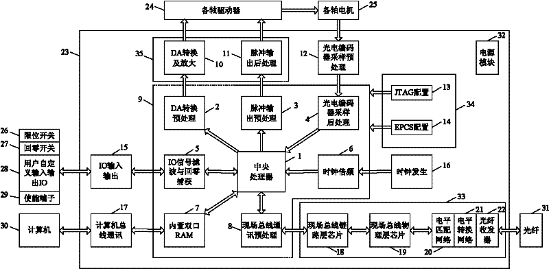
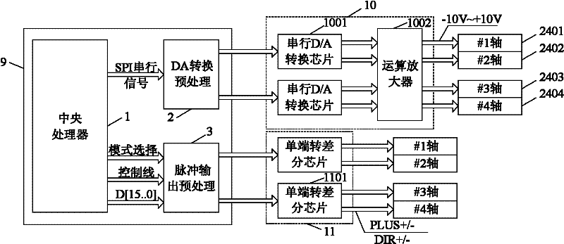
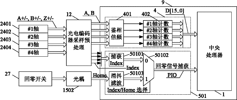
[0020] Such as figure 1 As shown, this embodiment includes: FPGA control module 9, PCI communication module 17, IEEE 1394 field bus optical fiber communication module 33, D/A conversion amplifier 10 and pulse output post-processing module 11, photoelectric encoder sampling pre-processing module 12, IO input and output module 15, power supply module 32, clock generation module 16, FPGA control module configuration module 34 and so on. Among them, FPGA control module 9 includes the following main parts: central processing unit 1, D/A conversion preprocessing module 2, pulse output preprocessing module 3, photoelectric encoder sampling post-processing module 4, IO signal filtering and return Zero capture module 5, clock multiplication module 6, built-in dual-port RAM module 7, IEEE 1394 bus communication preprocessing module 8.
[0021] The core of the FPGA control module 9 is the Cyclone series FPGA control module chip of Altera. The internal central processing unit 1 is constructed by the SOPC of the FPGA control module, and the remaining 7 modules are constructed by hardware programming languages or schematic diagrams. The central processing unit module 1 is the controller of the entire motion control system. Its function is to complete four-axis closed-loop control calculation, actual position sampling and latching, limit signal, zero return signal, enable signal, and user-defined input and output IO The signal capture and drive, respond to the command of the host computer and the analog voltage or pulse control of the motor. When the motion control system is used as an IEEE 1394 master node, the central processing unit 1 obtains the axis control reference values issued by the computer 30 from the built-in dual-port RAM module 7 through the PCI communication module 17, and reads from the IEEE 1394 communication preprocessing module 8. Get the current actual position of each axis, after PID closed-loop calculation, the speed control value is sent to each sub-node through the IEEE 1394 communication preprocessing module 8. When the motion control system is used as a child node, the central processing unit 1 obtains the current actual position of each axis from the photoelectric encoder post-processing module 4 and uploads it to the master node through the IEEE 1394 communication preprocessing module 8 for closed-loop calculation, and then from the IEEE The 1394 communication preprocessing module 8 obtains the motor control instructions issued by the master node, and then sends it to the servo driver through the D/A conversion preprocessing module 2 or the pulse output preprocessing module 3, thereby driving the motor to run. Regardless of whether it is used as a master node or a child node, the central processing unit 1 periodically accesses the IO signal filtering and zero return capture module 5. On the one hand, the output IO signal is output through 5, and on the other hand, it is continuously read by 5 latched Data acquisition limit signal, zero return signal, and each input IO signal. The central processing unit 1 receives the multiplied clock signal from the clock multiplication module 6 as a clock source.
[0022] In the FPGA control module 9, the D/A conversion preprocessing module 2 is connected to the central processing unit 1 through an SPI serial interface, and specifically includes three signal lines: SDO data output, SCK clock and CS chip selection. Among them, SCK is the clock signal of the central processing unit, SDO is the four-axis control data signal sent by the central processing unit 1 to the serial D/A chip, and CS is the chip selection signal for the module 2. When used as a child node, the central processing unit 1 sends the control data signals of the four axes to the D/A conversion preprocessing module 2 in each servo cycle, and the D/A conversion preprocessing module 2 analyzes the series of each axis according to the clock signal. The row control signal is divided, and finally the frame signal and data signal corresponding to each axis are generated. The generated frame signal and data signal, together with the clock signal, are finally output to the D/A conversion and amplification module 10 for D/A conversion.
[0023] In the FPGA control module 9, the pulse output preprocessing module 3 is connected to the central processing unit 1 through the following signal lines: parallel data line D[15..0], chip selection signal line CE[3..0], mode selection signal Line MODE[1..0]. Among them, the parallel data line D[15..0] transmits the data signal from the central processing unit 1 when the chip select signal line CEx is valid, CE[3..0] represents the chip select signal of #4-#1 four-axis, The output level of the mode selection signal line MODE[1..0] represents the pulse output mode control: MODE0=0, MODE1=0, it is the pulse output form of command pulse PULSE+direction DIRECTION; MODE0=1, MODE1=0, then It is the pulse output form of forward CW pulse/reverse CCW pulse; MODE0=0, MODE1=1, it is the 2-phase command pulse output form of A-phase pulse train + B-phase pulse train. The pulse output preprocessing module 3 obtains the multiplied clock signal from the clock multiplication module 6, and converts the obtained parallel data into a pulse sequence of the same frequency, and then outputs it to the pulse output post-processing module 11 for single-ended signal to differential Signal conversion.
[0024] In the FPGA control module 9, the photoelectric encoder sampling post-processing module 4 is connected to the central processing unit 1 through the following signal lines: parallel data line D[15..0], chip selection signal line EncoderCE[3..0]. When the chip select signal line EncoderCEx is valid, the actual position sampling of the x-axis is transmitted from the photoelectric encoder post-processing module 4 to the central processing unit 1. This module is used to discriminate and multiply the frequency of the external photoelectric encoder signal and accumulate the count.
[0025] In the FPGA control module 9, the limit switch, enable terminal, and return switch signals in the IO signal filtering and zero return capture module 5 are connected to the central processing unit 1 through PIO, and the user-defined input and output signals are passed through the parallel data line D[15..0] and chip selection signal line ExinpCE, ExoutpCE are connected with the central processing unit 1. The central processing unit 1 directly reads the state of the limit switch and the zero return signal after debounce and filtering through the PIO, and latches and outputs the enable signal through the PIO. The central processing unit 1 reads the latched state of the user-defined input IO to the data bus D[15..0] by controlling the state of the ExinpCE and ExoutpCE signal lines, or sends the data of D[15..0] to Output IO.
[0026] In the FPGA control module 9, the clock multiplication module 6 is a phase-locked loop PLL. The input of the clock multiplication module 6 is a 50MHz clock signal from the clock generator 16-active crystal oscillator, and the phase-locked loop multiplies the clock signal by 4 to obtain a 200MHz clock frequency as the clock signal input of the central processing unit 1.
[0027] In the FPGA control module 9, the built-in dual-port RAM module 7 is a dual-port RAM implemented by software. The module has a 1K×16bit memory space, is connected to the central processing unit through the Avalon bus, and is connected to the PCI 9052 of the computer bus communication module 17 through the data line, address line and control line. The dual-port RAM can be accessed by the central processing unit or PCI9052 to realize data interaction between the two parties.
[0028] In the FPGA control module 9, the IEEE 1394 communication preprocessing module 8 is connected to the central processing unit through the Avalon bus. At the beginning of power-on, the central processing unit 1 configures and initializes the external IEEE 1394 link layer chip 18 through the IEEE 1394 communication preprocessing module 8. When the system receives a data packet from another node, the IEEE 1394 communication preprocessing module 8 reads the IEEE 1394 link layer chip 18 to obtain the data signal sent by the other node, and then returns the confirmation packet, and unpacks the data packet to obtain it. The effective transmission data is then transmitted to the central processing unit 1. When the system sends data packets to other nodes, the IEEE 1394 communication preprocessing module 8 automatically packs the transmission data received from the central processing unit 1, and adds the header information before the data packet, and then sends the data packet to the designated The node then waits for the return of the confirmation data packet, and thus completes a sending cycle.
[0029] in figure 2 In the illustrated embodiment, the D/A conversion and amplification module 10 includes two serial D/A conversion chips 1001 and an operational amplifier 1002. The pulse output post-processing module 11 includes two single-ended signal-to-differential signal chips 1101. The D/A conversion chip 1001 obtains the frame signal, the data signal and the clock signal from the D/A conversion preprocessing module 2, and converts it into the control analog voltage signal of the four axes, and sends the voltage signal to the operational amplifier with four channels The chip 1002 is amplified into an analog voltage signal of -10V~+10V, and then sent to the servo drivers 2401, 2402, 2403, and 2404 of each axis. The single-ended signal-to-differential signal chip 1101 obtains a single-ended pulse signal from the pulse output preprocessing module 3, which is converted into a differential signal by the pulse output module 11, and the signal is used to drive the pulse input servo drivers 2401, 2402, 2403, 2404.
[0030] in image 3 In the illustrated embodiment, the photoelectric encoder differential signals A+/-, B+/-, and Z+/- of each axis servo driver 2401, 2402, 2403, 2404 are sent to the photoelectric encoder sampling preprocessing module 12 for differential signals to single-ended Signal conversion. The converted A and B signals enter the post-sampling processing module 4 of the photoelectric encoder of the FPGA control module for phase discrimination, frequency multiplication and counting. The phase discrimination and frequency multiplication module 401 performs 2 or 4 multiplication on the encoder signal according to the phases of the A and B signals and the frequencies of the A and B signals. The multiplied signal enters the counting module 402 for accumulation and counting. The counted value is read by the central processing unit 1 in each sampling period. The index signal, the Z-phase signal converted from a differential signal to a single-ended signal, becomes a capture signal after passing through the capture Index module 50101. Using the Index/Home signal selection module 50102, the zero return signal will select one of the Index signal and the Home switch signal, and finally send it to the central processing unit 1. For the capturing Index module 50101, when the Index signal of each axis changes from low to high, the Index signal of the corresponding axis is captured and transmitted to the Index/Home signal selection module 50102. The Index/Home signal selection module 50102 has a selection control line "Index/Home selection". When the input level of the control line is low, the Home signal will enter the central processing unit 1 through this module. When the input level is high, The Index signal will enter the CPU 1 through this module. For the anti-interference filtering module 50103, it mainly filters the zero return switch signal. When the switch signal remains unchanged within a certain time range, the corresponding switch signal will enter the Index/Home signal selection module 50102.
[0031] in Figure 4 In the illustrated embodiment, the limit switch 26 signal, the zero return switch 27 signal, and the user-defined input 2801 signal enter the FPGA control module 9 after passing through the IO input module 1501 (subordinate to the IO input and output module 15), and first perform the anti-interference filter Debounce filtering is performed in the module 50103. The filtered limit signal enters the central processing unit 1 through the PIO interface; and the user-defined input signal after the anti-interference filtering will enter the central processing unit 1 through the data bus D[15..0]. On the other hand, the central processing unit 1 outputs the user-defined output signal to the IO output module 1502 (subordinate to the IO input and output module 15) through the data bus D[15..0], and then transmits the signal to the user-defined output Terminal 2802: The central processing unit 1 transmits the enable signal to the IO output module 1502 through the PIO channel, and then transmits the signal to the enable terminal 29.
[0032] in Figure 5 In the illustrated embodiment, when used as a master node or independently used as a PCI-based motion control system, the board and the computer are connected through PCI. The computer can be an industrial control computer or an embedded computer 3001, and the physical interface form of the PCI protocol can be a PCI golden finger or a PC104Plus pin 3002. The computer 30 directly accesses the PCI communication module 17, and the PCI 9052 chip in the PCI communication module 17 maps the local bus address to the computer access space. The FPGA control module 9 has a built-in dual-port RAM7. The dual-port RAM7 is connected to the central processing unit 1 through the Avalon bus, and is connected to the PCI 9052 chip through the PCI 9052 local bus. Both the central processing unit 1 and the PCI 9052 chip can implement access to the built-in dual-port RAM module 7 so as to implement data interaction between the computer 30 and the motion control system 23.
[0033] in Image 6 In the illustrated embodiment, the IEEE 1394 communication structure includes the following parts: FPGA control module 9, IEEE 1394 link layer chip 18, IEEE 1394 physical layer chip 19, IEEE 1394 communication level matching network 20, and IEEE 1394 level conversion network 21. IEEE 1394 communication optical fiber transceiver 22 and communication optical fiber 31. The FPGA control module internal and IEEE1394 communication related modules include the central processing unit 1 and the IEEE 1394 communication preprocessing module 8. The IEEE 1394 communication preprocessing module 8 is connected to the central processing unit 1 through the Avalon bus, and is connected to the IEEE 1394 link layer chip through the data bus, address bus, and control line. The IEEE 1394 communication preprocessing 8 obtains data from the central processing unit 1, and then adds information such as a packet header and writes the data packet to the IEEE 1394 link layer chip 18. At the same time, the IEEE 1394 communication preprocessing 8 interrupts the reading of the IEEE 1394 link layer chip 18 to obtain the data sent by other nodes, and then unpacks the valid data from it, and sends the data to the central processing unit 1.