Variable-temperature microscopic magnetic photoelectric testing system with flexible measuring geometry

An optoelectronic testing and geometric technology, which is applied in measurement devices, color/spectral property measurement, fluorescence/phosphorescence, etc.

Inactive Publication Date: 2011-04-20
INST OF SEMICONDUCTORS - CHINESE ACAD OF SCI
View PDF0 Cites 12 Cited by
  • Summary
  • Abstract
  • Description
  • Claims
  • Application Information

AI Technical Summary

Problems solved by technology

[0004] Keeping the sample in a low-temperature environment is also one of the necessary conditions for observing significant spin-correlation effects: the spin polarization of the electrons in the sample, that is, the number of electrons with +1 / 2 and -1 / 2 spins is different, is a The non-equilibrium state always tends to relax to the balanced non-polarized state, and the increase in temperature will accelerate this relaxation process, making it difficult or even impossible to observe the spin polarization effect

Method used


Image

  • Variable-temperature microscopic magnetic photoelectric testing system with flexible measuring geometry
  • Variable-temperature microscopic magnetic photoelectric testing system with flexible measuring geometry
  • Variable-temperature microscopic magnetic photoelectric testing system with flexible measuring geometry

Examples


Embodiment Construction

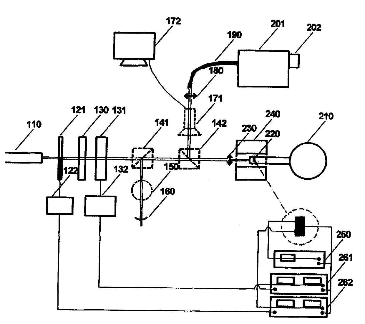
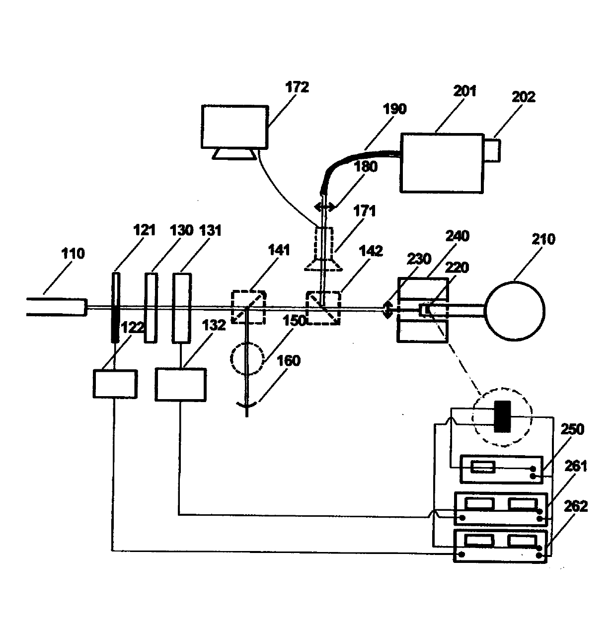
[0032] The invention is a set of temperature-variable micro-magneto-optical test system with flexible measuring geometry.

[0033] First introduce the composition of this system in detail, please refer to figure 1 As shown, the system includes:

[0034] A titanium-doped sapphire laser 110, used to excite the sample 220, a chopper 121, a broadband linear polarizer 130, a photoelastic modulator 131, and a first broadband depolarizer are arranged in sequence on the outgoing optical path of the titanium-doped sapphire laser 110 Dichroic prism 141 , second broadband depolarizing dichroic prism 142 , first objective lens 230 and liquid nitrogen Dewar 210 .

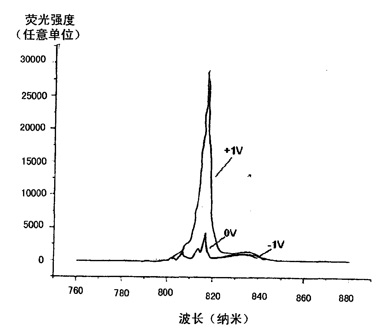
[0035] The emission wavelength of the titanium-doped sapphire laser 110 is adjustable within the range of 700-1030 nanometers, so that various behaviors of carriers with different energies in the sample 220 can be studied.

[0036] The chopper 121 is connected to a controller 122 for light intensity modulation of the excitatio...


PUM


Abstract

The invention relates to a set of variable-temperature microscopic magnetic photoelectric testing system with flexible measuring geometry, which comprises a titanium-doped sapphire laser as well as a chopper, a wide waveband linear polarizing film, a photoelastic modulator, a first wideband depolarization beam splitting prism, a second wideband depolarization beam splitting prism, a first objective lens and a liquid nitrogen Dewar which are arranged on the emergent light path of the titanium-doped sapphire laser in sequence, wherein the refracted light path of the second wideband depolarization beam splitting prism also comprises a camera and a display connected with the same, a second object lens is arranged on the light path behind the camera, and a monochromator and a matched detector are connected behind the second object lens through optical fibers; the chopper is connected with a controller; the photoelastic modulator is connected with a controller; the refracted light path of the first wideband depolarization beam splitting prism also comprises a lighting source and a detector; the refracted light path of the second wideband depolarization beam splitting prism also comprises the camera and the display connected with the camera; a neodymium iron boron permanent magnet is coaxially sheathed on the front end of the liquid nitrogen Dewar in a contactless mode; and the system also comprises a DC current source, and two output ports of the DC current source are connected with a sample through conducting wires.

Description

technical field [0001] The invention relates to the field of semiconductor spintronics, in particular to the measurement of spin-related energy band structures and transport properties of semiconductor spintronics materials (such as ferromagnetic metal / semiconductor structures, dilute magnetic semiconductors, etc.). Background technique [0002] Since the giant magnetoresistance (Giant Magneto Resistance) effect was discovered in the Fe / Cr multilayer structure in 1988, in the past 20 years, another intrinsic property of electrons, spin, has been used to act as electron charges. It is similar in the field of modern information technology. The new subject of the role of spintronics, both in the laboratory and in the industry, has made amazing developments. [0003] In the study of spintronics, the magnetic field is often an indispensable experimental condition: for the so-called dilute magnetic semiconductors such as gallium manganese arsenic, due to the existence of the Zeema...

Claims


Application Information

Patent Timeline
Patent Type & Authority Applications(China)
IPC IPC(8): G01N21/39G01N21/64G01N21/66G01N21/19
Inventor 吴昊郑厚植朱汇李韫慧
Owner INST OF SEMICONDUCTORS - CHINESE ACAD OF SCI
Why Eureka
Try Eureka