Array type light evening device with annulus photon screen and manufacturing method thereof

A photon sieve and homogenizer technology, which is applied in the field of laser beam wavefront shaping, can solve the problems of large transmission loss, cost reduction, and high requirements for designers

Inactive Publication Date: 2011-04-20
INST OF MICROELECTRONICS CHINESE ACAD OF SCI
View PDF0 Cites 8 Cited by
  • Summary
  • Abstract
  • Description
  • Claims
  • Application Information

AI Technical Summary

Problems solved by technology

The kaleidoscope method is easy to manufacture and adjust, the cost is greatly reduced, and the size of the output spot can be easily changed, but the transmission loss of this system is relatively large
[0008] Cylindrical mirror method: The principle of the method is to form a hollow square structure surrounded by four cylindrical mirrors. Each cylindrical mirror is installed on a fine adjustment frame. The size and shape of the hollow part can be controlled through adjustment. The laser is irradiated on the device Above, the hollow part of the laser passes through directly, and the light irradiated on the edge cylindrical lens will compensate for the weak light intensity part of the middle light. By calculating the parameters of the cylindrical lens and adjusting the adjustment knob properly, the uniform light effect can be obtained. The advantage of this method is that the beam transmittance is higher and the uniform light effect is better, but the designer has higher requirements, and the designer needs to calculate the lens parameters and design a high-precision fine-tuning mechanism

Method used


Image

  • Array type light evening device with annulus photon screen and manufacturing method thereof
  • Array type light evening device with annulus photon screen and manufacturing method thereof
  • Array type light evening device with annulus photon screen and manufacturing method thereof

Examples


Embodiment Construction

[0037] In order to make the object, technical solution and advantages of the present invention clearer, the present invention will be further described in detail below in conjunction with specific embodiments and with reference to the accompanying drawings.

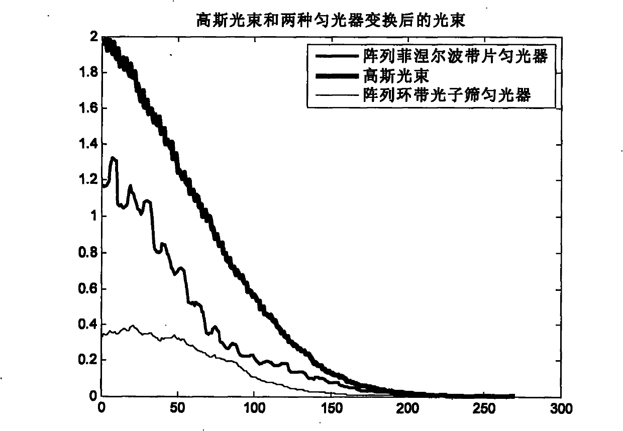
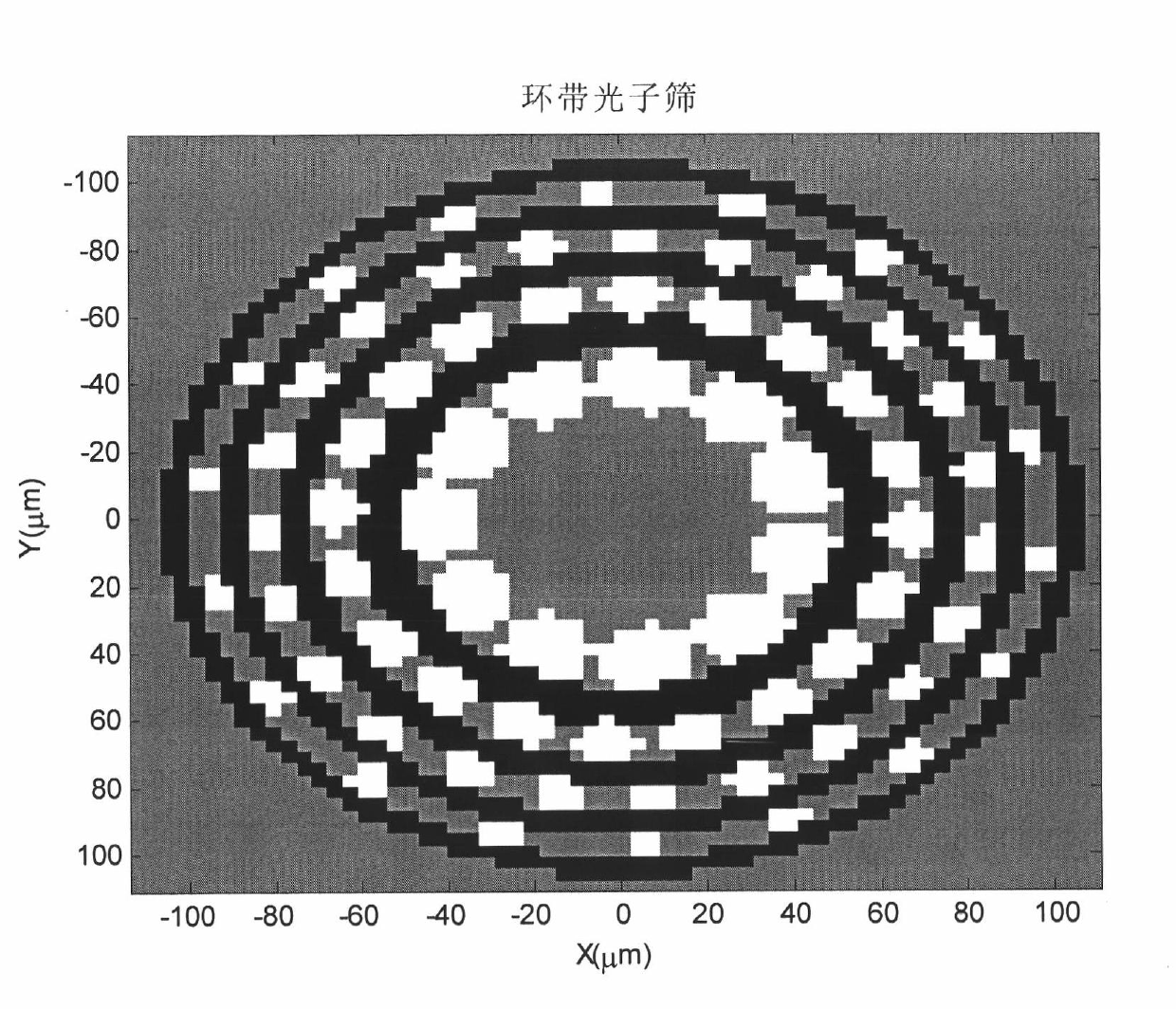
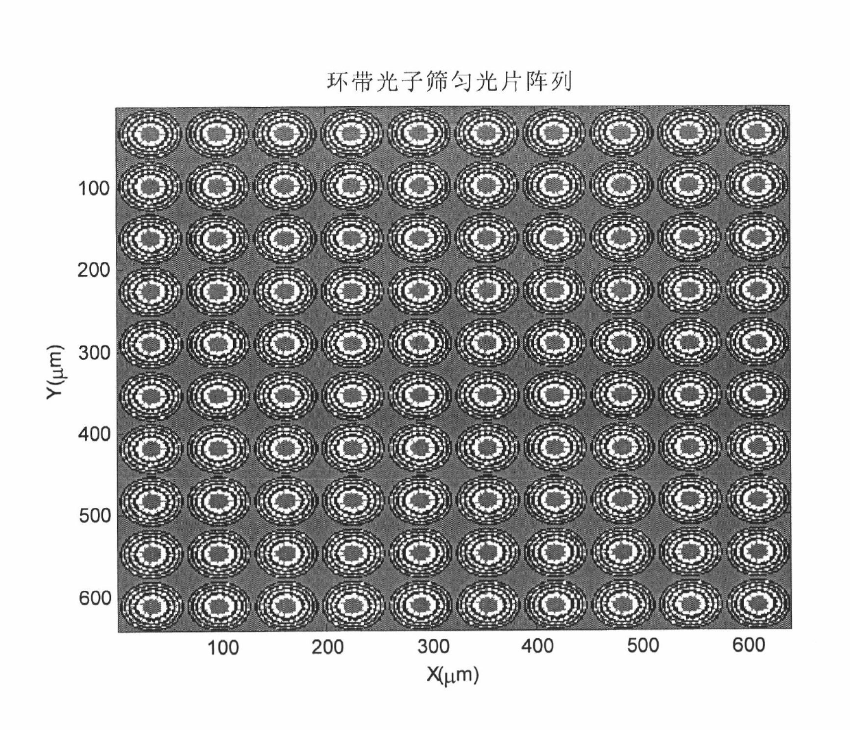
[0038] Array annular photon sieve homogenizer is a new type of diffractive optical phase element, that is, phase plate. The phase plate is placed before or after the diffraction-limited lens to correct the far-field diffraction light field of the laser beam, that is, to homogenize the light, and to achieve a diffracted beam that is closer to the plane wavefront than the irregular wavefront of the incident beam (such as a Gaussian beam). The invention provides the design structure of the photon sieve homogenizer with an array ring, and carries out related simulation experiments. Experiments have verified that the wavefront flattening of Gaussian beams can be achieved by using the array annular photon sieve homogenizer, tha...


PUM

PropertyMeasurementUnit
thicknessaaaaaaaaaa
refractive indexaaaaaaaaaa

Abstract

The invention discloses an array type light evening device with an annulus photon screen and a manufacturing method thereof. The array type light evening device with the annulus photon screen is an annulus photon screen array which is manufactured on a transparent medium, and the annulus photon screen is used as a basic unit of the array. The annulus photon screen is formed by a plurality of homocentric diffractive hole annuluses and a plurality of homocentric etching ring annuluses, which are alternately nested, and the diffractive hole annulus is the closest to the center of the annulus photon screen; the width of the diffractive hole annulus and the width of the etching ring annulus are gradually decreased respectively from the center of the annulus photon screen to outside, the width of the diffractive hole annulus is equal to the width of the etching ring annulus which is adjacent to the diffractive hole annulus far from the central direction of the annulus photon screen, and the size of each light penetrating hole is the same as the width of the corresponding etching phase annulus. By using the invention, gauss beams and other wavefront uneven laser beams are transformed into wavefront diffractive beams which are approximate planes.

Description

technical field [0001] The invention relates to the technical field of wavefront shaping of laser beams, in particular to a wavefront flattening of a Gaussian wavefront and an irregular wavefront laser beam in the far-field diffraction light field, that is, to realize a light field close to a plane wavefront distribution An array ring-band photon sieve homogenizer and a manufacturing method thereof. The array annular photon sieve homogenizer can be used in beam shaping, microelectronics maskless etching and other various optical paths that require a plane wave front. Background technique [0002] It is a practical subject to homogenize the laser beam with Gaussian wavefront and irregular wavefront through various ways, so that the beam can be transformed into a beam close to the plane wavefront, and it has a wide range of applications in various optical paths, such as in beam shaping , Microelectronics maskless lithography and other various instruments that require a planar...

Claims


Application Information

Patent Timeline
Patent Type & Authority Applications(China)
IPC IPC(8): G02B27/09G02B5/18G02B27/42G03F7/20G03F7/36
Inventor 贾佳谢长青刘明
Owner INST OF MICROELECTRONICS CHINESE ACAD OF SCI
Why Eureka
Try Eureka