Manufacturing method of oxide layer between splitting grids

A manufacturing method and gate oxide layer technology, which is applied in semiconductor/solid-state device manufacturing, electrical components, circuits, etc., can solve problems such as thick oxide layer, inability to meet process requirements, serious smile effect, etc., achieve short process time, improve Smile effect, avoiding the effect of excessively thick oxide layer

Inactive Publication Date: 2011-04-20
SEMICON MFG INT (SHANGHAI) CORP +1
View PDF1 Cites 6 Cited by
  • Summary
  • Abstract
  • Description
  • Claims
  • Application Information

AI Technical Summary

Problems solved by technology

[0006] The invention solves the problem that the oxide layer formed between the split gates in the prior art is too thick to meet the process requirements and the smile effect is serious

Method used


Image

  • Manufacturing method of oxide layer between splitting grids
  • Manufacturing method of oxide layer between splitting grids
  • Manufacturing method of oxide layer between splitting grids

Examples


Embodiment approach

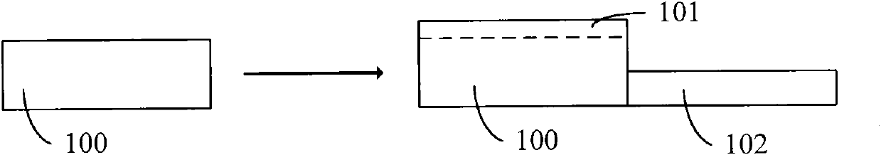
[0016] For this reason, the manufacturing method of the oxide layer between the split gates of the present invention adopts a rapid thermal process to grow the oxide layer in the ion implantation region. According to an embodiment of the present invention, it includes: using rapid thermal process (RTP, Rapid Thermal Process) equipment to perform in-situ steam generation (ISSG, In-Situ Steam Generation), so that the surface of the common source region between the split gates form an oxide layer.

[0017] The method of in-situ water vapor generation grows an oxide layer through a high-temperature water vapor atmosphere, and the growth rate of the oxide layer is relatively fast. Moreover, the rapid thermal process equipment has a fast heating and cooling speed. At the same time, the rapid thermal process equipment is a single-wafer process equipment. Compared with the situation where the furnace tube oxidation is usually dozens of wafers, the gas source that the wafers in the rap...


PUM


Abstract

The invention relates to a manufacturing method of an oxide layer between splitting grids, which comprises the following step of: carrying out in-situ vapor generation by using a rapid thermal processing device so as to form the oxide layer on the surface of a common source region between the splitting grids. The manufacturing method can accurately control the thickness of the oxide layer formed on the highly doped common source region so as to avoid over thickness of the oxide layer. Moreover, the thickness of the formed oxide layer is uniform, and the smiling effect is improved.

Description

technical field [0001] The invention relates to the technical field of memory manufacturing, in particular to a manufacturing method of an oxide layer between split gates. Background technique [0002] Flash memory generally adopts a multilayer gate type memory cell structure. refer to figure 1 As shown, the memory cell transistor with a multilayer gate structure has a floating gate 14 in addition to a drain 11 , a source 12 and a gate 13 . Data storage is achieved by controlling the amount of charge stored in the floating gate 14 (floating gate) of the memory cell transistor. For memory cell transistors with this structure, if the floating gate is unstable, "over erase" will occur. [0003] In view of this, the prior art provides corresponding solutions, for example with reference to figure 2 As shown, Sanyo Semiconductor proposed a split-gate memory cell structure. In the split gate structure, the drain 21 and the source 22 are split, and the gate 23 has a structure ...

Claims


Application Information

Patent Timeline
Patent Type & Authority Applications(China)
IPC IPC(8): H01L21/285
Inventor 涂火金沈忆华宋化龙李亮
Owner SEMICON MFG INT (SHANGHAI) CORP
Why Eureka
Try Eureka