Protection device and method for semiconductor apparatus

A technology for protecting devices and semiconductors, which is applied in the fields of semiconductor devices, semiconductor/solid-state device manufacturing, semiconductor/solid-state device components, etc., to achieve the effect of convenient process and simple structure

Inactive Publication Date: 2011-04-20
SEMICON MFG INT (SHANGHAI) CORP
View PDF0 Cites 11 Cited by
  • Summary
  • Abstract
  • Description
  • Claims
  • Application Information

AI Technical Summary

Problems solved by technology

Due to the existence of the protection diode, when a negative voltage is applied to the gate of the NMOS transistor (that is, the accumulation mode), the applied negative voltage will be released to the ground through the protection diode 102, so the NMOS transistor in the accumulation mode cannot be measured

Method used


Image

  • Protection device and method for semiconductor apparatus
  • Protection device and method for semiconductor apparatus
  • Protection device and method for semiconductor apparatus

Examples


Embodiment Construction

[0022] In the following description, numerous specific details are given in order to provide a more thorough understanding of the present invention. It will be apparent, however, to one skilled in the art that the present invention may be practiced without one or more of these details. In other examples, some technical features known in the art are not described in order to avoid confusion with the present invention.

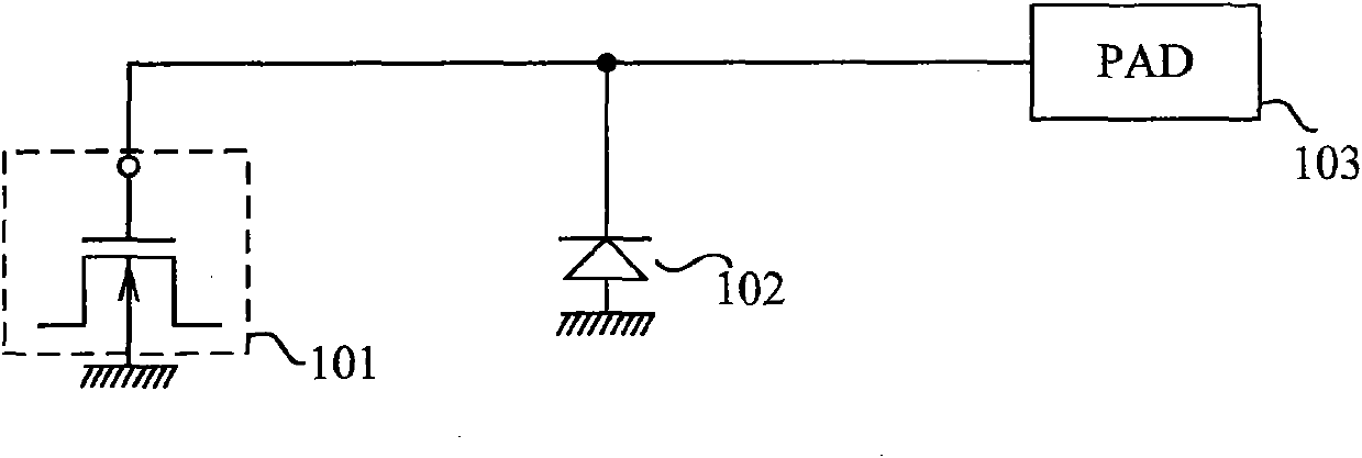
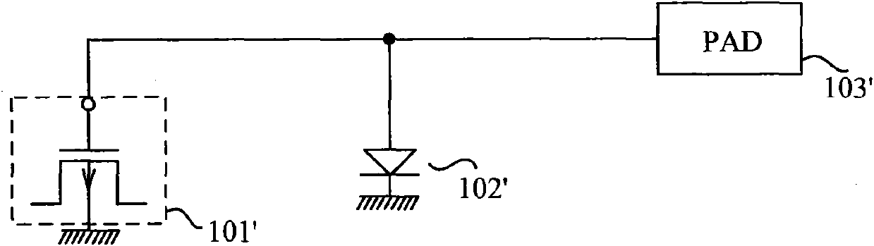
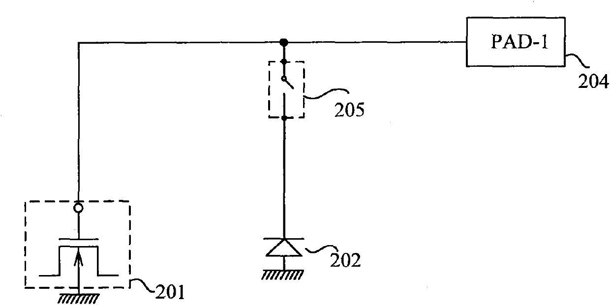
[0023] Figure 2a with Figure 2b The improved NMOS device circuit and the protection circuit of the PMOS device circuit according to the present invention are respectively shown. The protection circuit according to the invention can not only eliminate the influence of plasma damage generated in the manufacturing process stage, but also ensure that the MOS device can be tested in both the reverse mode and the accumulation mode in the subsequent device test stage. As shown in the figure, the present invention connects a switching element between the protection...


PUM


Abstract

The invention provides a protection device for a semiconductor apparatus, which comprises a transistor, a first pad connected to the grid of the transistor, and a switch element and a diode in turn connected between the ground and the join point of the first pad and the grid of the transistor. The protection device of the invention can be used for protecting the semiconductor apparatus, particularly for preventing MOS transistor from being damaged by plasma in the manufacturing process and for testing the MOS elements under reverse mode and accumulating mode.

Description

technical field [0001] The present invention relates to semiconductor devices, in particular to a circuit protection device for protecting semiconductor devices from plasma damage (PID). Background technique [0002] As the semiconductor manufacturing process enters the deep submicron stage, the plasma process has become an increasingly widely used process technology. Plasma technology is mainly used in the fields of ultraviolet lithography, plasma etching and ion implantation. However, due to the operation of plasma in the manufacturing process of semiconductor devices, plasma damage inevitably occurs. Plasma damage can damage semiconductor devices, especially the gate oxide layer and device characteristics of MOS devices, resulting in reduced device performance. For example, the threshold voltage of the MOS device drifts, and the breakdown charge and breakdown voltage of the gate oxide film change, resulting in the transition of minority carriers in the conductive channe...

Claims


Application Information

Patent Timeline
IPC IPC(8): H01L27/02H01L23/60H01L21/82H02H9/00
Inventor 吴启熙
Owner SEMICON MFG INT (SHANGHAI) CORP
Why Eureka
Try Eureka