Nonvolatile memory and arrangement thereof

A non-volatile storage and non-volatile technology, applied in the direction of electrical components, electrical solid-state devices, semiconductor devices, etc., can solve the problems of high cost, complex process, poor component yield, etc., to increase component density, The effect of improving device performance and reducing leakage current

Active Publication Date: 2011-04-27
UNITED MICROELECTRONICS CORP
View PDF3 Cites 0 Cited by
  • Summary
  • Abstract
  • Description
  • Claims
  • Application Information

AI Technical Summary

Problems solved by technology

However, in the advanced logic process, the process of using double-layer polysilicon non-volatile memory as embedded memory is complex and costly, and the component yield is not good

Method used


Image

  • Nonvolatile memory and arrangement thereof
  • Nonvolatile memory and arrangement thereof
  • Nonvolatile memory and arrangement thereof

Examples


Embodiment Construction

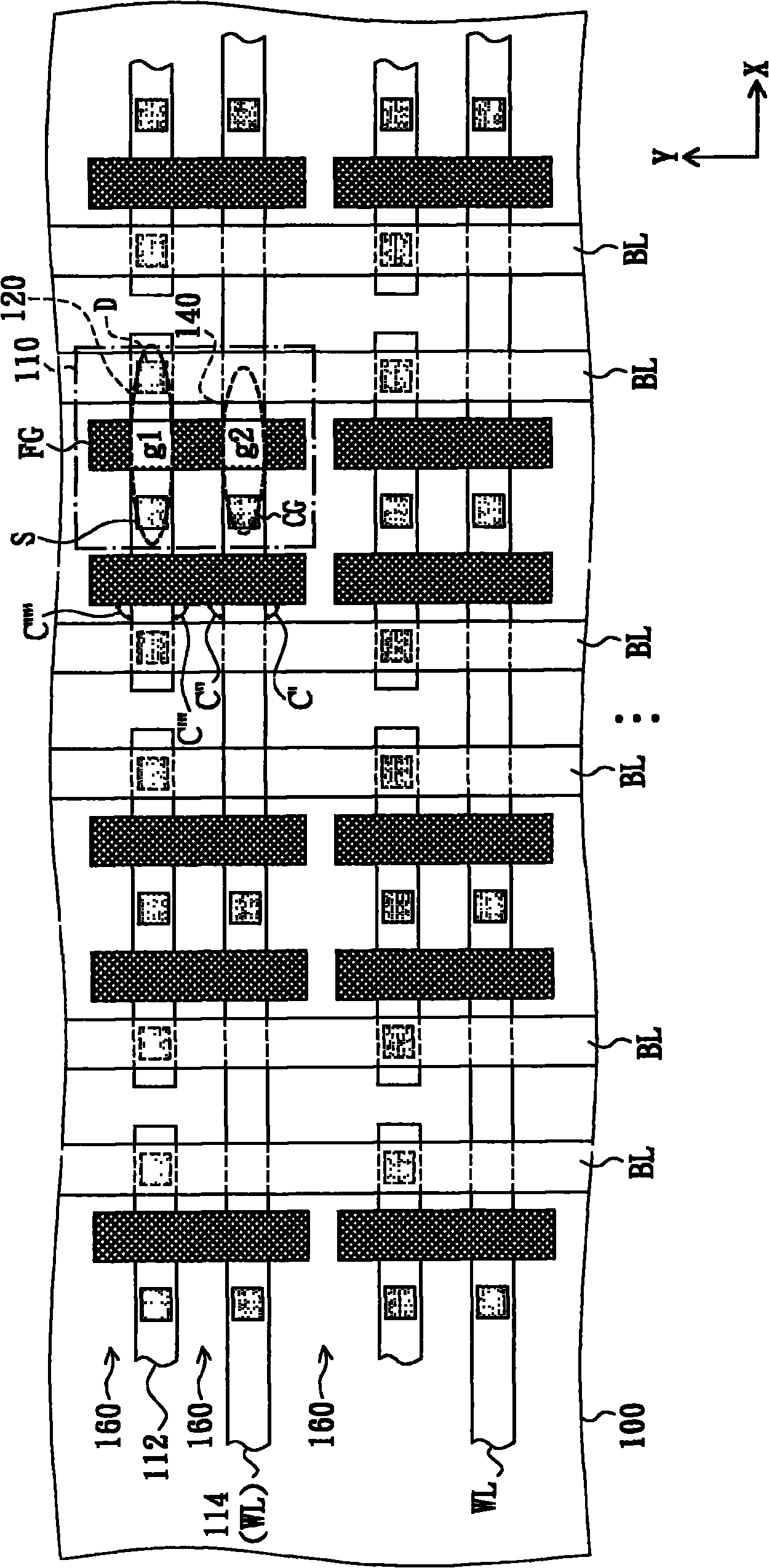
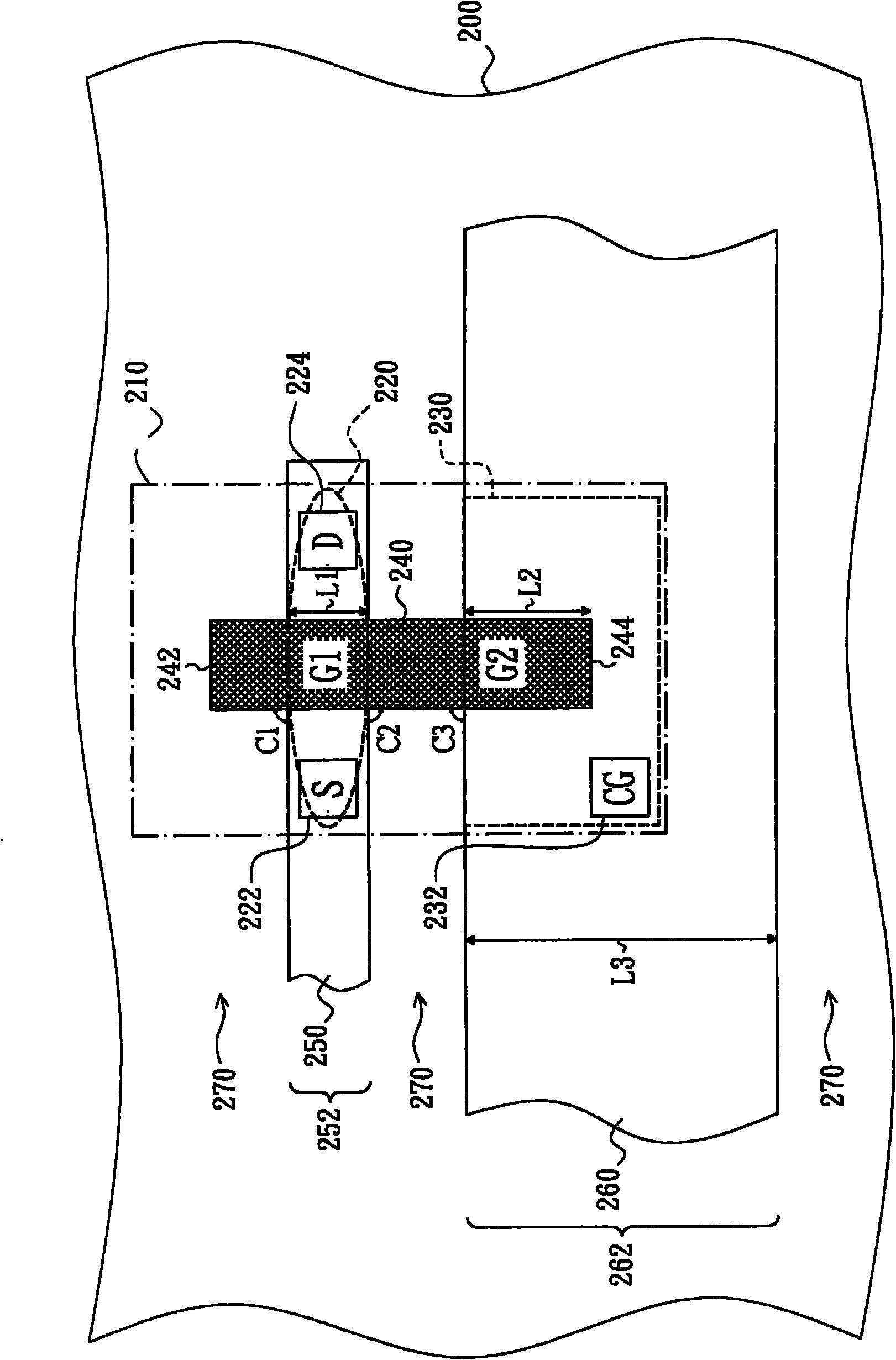
[0063] figure 2 It is a schematic top view of a non-volatile memory unit according to an embodiment of the present invention.

[0064] Please refer to figure 2 , the non-volatile memory unit 210 of the present invention is composed of a semiconductor substrate 200, a conductor 240, a plurality of isolation structures 270, a first-type doped well 260, two first ion-doped regions 222, 224 and a second ion-doped impurity region 232.

[0065] A plurality of isolation structures 270 parallel to each other are disposed in the semiconductor substrate 200 , such as shallow trench isolation structures (Shallow Trench Isolation, STI). These isolation structures 270 partition the semiconductor substrate 200 into transistor regions 252 and capacitor regions 262 parallel to each other. The first-type doped well 260 is disposed in the container region 262 and is, for example, an N-type doped well.

[0066] In this embodiment, the semiconductor substrate 200 is, for example, an undoped...


PUM


Abstract

The invention discloses a nonvolatile memory and the arrangement thereof. In the nonvolatile memory unit, an isolation structure is arranged in a semiconductor base to isolate a transistor area and a capacitor area, a first type dopant well is arranged in the capacitor area, a conductor is crossed above the isolation structure, the transistor area and the first type dopant well and comprises a capacitance part and a transistor part, wherein the capacitance part is positioned above the first type dopant well, and the transistor part is positioned above the transistor area; the conductor is provided with a first side edge and a second side edge which are mutually opposite, the first side edge is positioned above the isolation structure of one side of the transistor area, the second side edge is positioned above the first type dopant well, in addition, two first iron doping areas are respectively arranged into the transistor areas of both sides of the transistor part and form a transistor with the transistor part, and a second iron doping area is arranged in the capacitor area outside the shade of the conductor and forms a capacitor with the capacitance part. According to the invention, drain current can be reduced.

Description

technical field [0001] The present invention relates to a semiconductor element and its layout structure, and in particular to a layout of a non-volatile memory unit and a non-volatile memory. Background technique [0002] The non-volatile memory (Non-Volatile Memory, NVM) device has the characteristic that the data stored in the device will not disappear due to the interruption of the power supply, so it has become one of the memory devices commonly used to store data at present. [0003] According to the limitation of the read and write times of the memory, non-volatile memory can be divided into: multi-time programmable memory (MTP memory) with repeatable read and write function and data that can only be provided once There are two types of one-time programmable memory (OTP memory) for writing. In addition, if it is distinguished from the device structure, it can be further divided into: double-poly non-volatile memory and single-poly non-volatile memory. [0004] Since...

Claims


Application Information

Patent Timeline
Patent Type & Authority Applications(China)
IPC IPC(8): H01L27/115H01L29/92H01L29/06H01L23/528
Inventor 施泓林陈智彬殷珮菁蔡慧芳
Owner UNITED MICROELECTRONICS CORP
Why Eureka
Try Eureka