Graph masking method for improving luminous efficiency of GaN base LED (light-emitting diode)

A technology of luminous efficiency and graphics, applied in electrical components, circuits, semiconductor devices, etc., can solve the problems of poor repeatability, complex process and high cost

Inactive Publication Date: 2011-04-27
YUTI LIGHTING SHANGHAI
View PDF0 Cites 23 Cited by
  • Summary
  • Abstract
  • Description
  • Claims
  • Application Information

AI Technical Summary

Problems solved by technology

Since most of the substrate materials currently used are sapphire, the etching process is complicated and the cost is high
Wet etching is also used, the cost is lower but the repeat controllability is poor
[0011] 4. The combination or deformation of the above two or several methods: using the graphic substrate method and the surface roughening method or using the graphic substrate method and the surface patterning method at the same time, the light extraction efficiency is improved more obviously, but the process is more complicated , costly

Method used


Image

  • Graph masking method for improving luminous efficiency of GaN base LED (light-emitting diode)
  • Graph masking method for improving luminous efficiency of GaN base LED (light-emitting diode)
  • Graph masking method for improving luminous efficiency of GaN base LED (light-emitting diode)

Examples


Embodiment 1

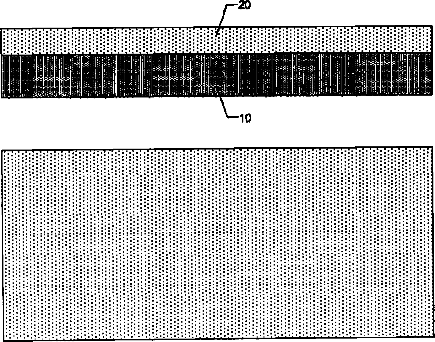
[0043] (a) if figure 1 As shown, a GaN single crystal thin film 20 with uniform thickness, flat and crack-free is grown on a sapphire substrate 10 by metal-organic vapor phase epitaxy (MOVPE). The thin film 20 has a thickness T=2000 nm.

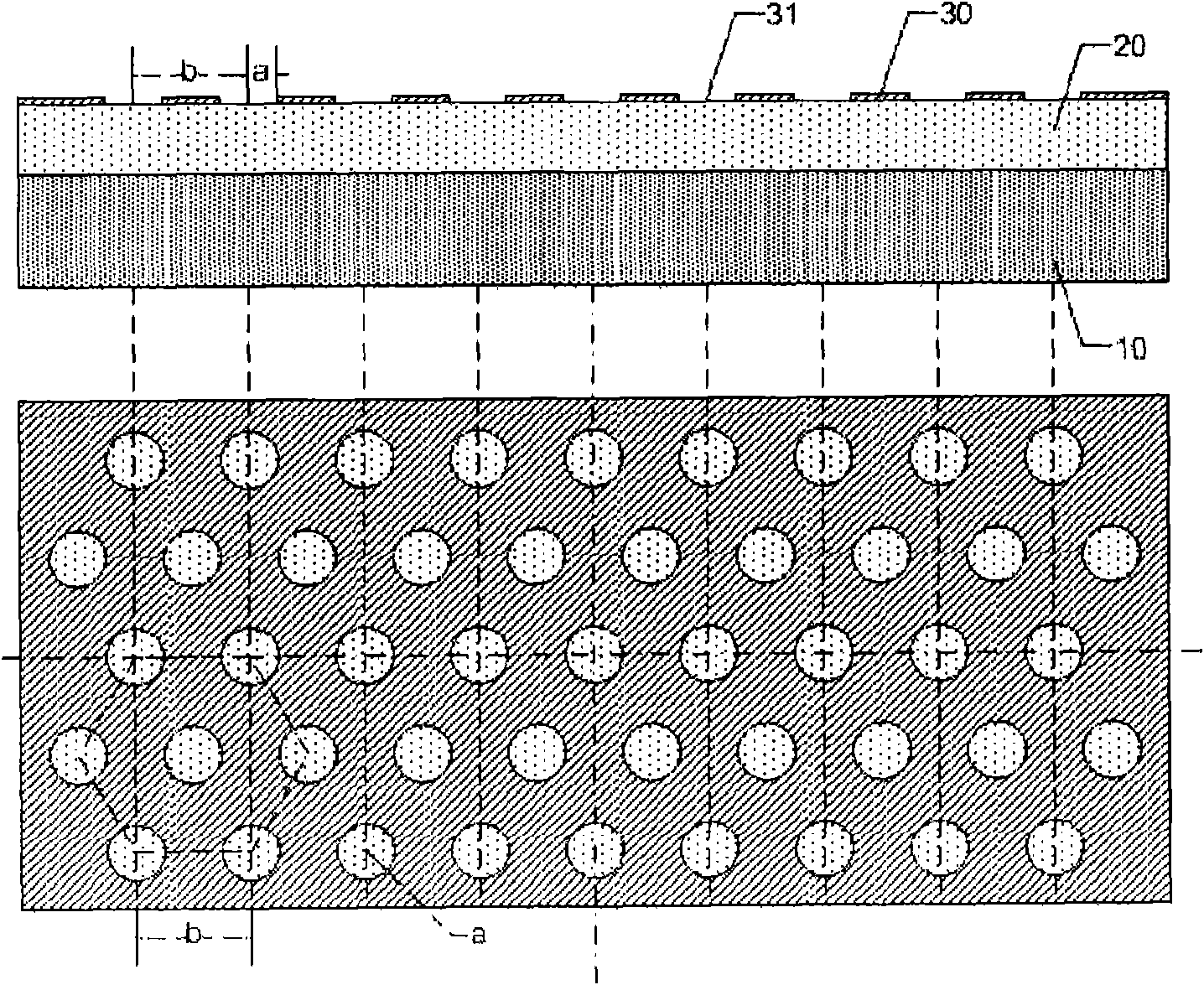
[0044] (b) if figure 2 As shown in A, a layer of photoresist mask 30 is evenly coated on the GaN thin film 20, and the thickness of the mask is c=5000nm. A regular hexagonal distribution pattern 31 is produced by using standard photolithography technology. The pattern 31 is a circular cavity with a radius a=1500nm and a minimum distance b=3000nm between adjacent circular cavities.

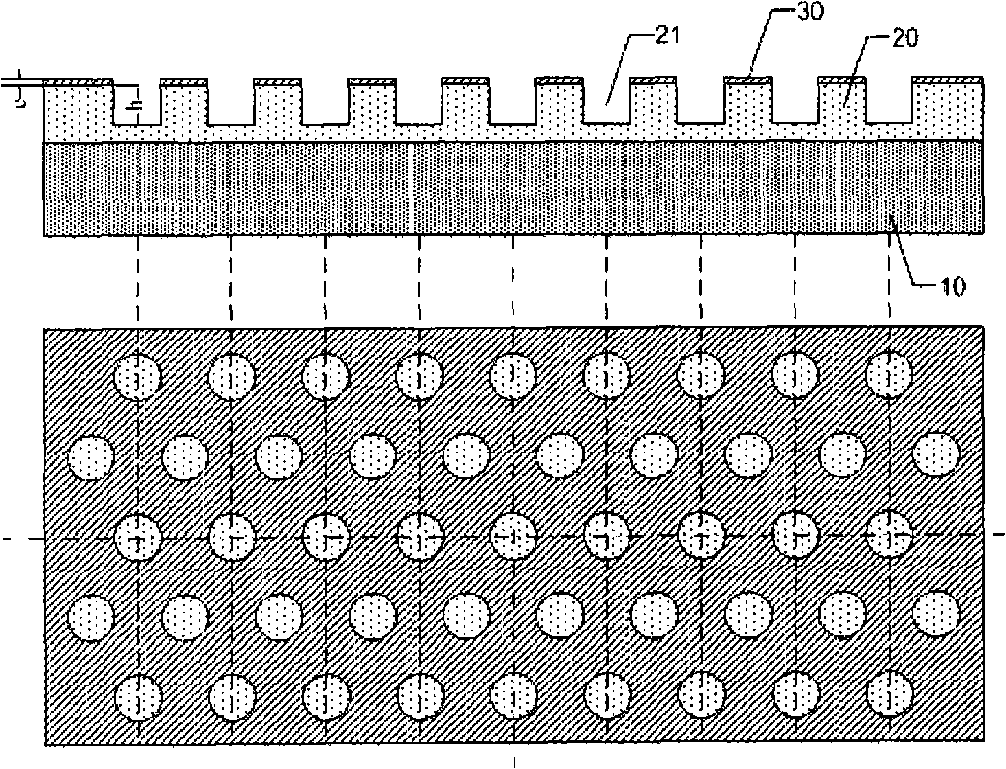
[0045] (c) if Figure 3A As shown, the GaN thin layer 20 is selectively etched using a mask 30 with regularly distributed patterns 31 . In this preferred embodiment using an inductively coupled plasma etching (ICP) method, the portion covered by the mask 30 is protected from etching, and the portion not covered by the mask 30 is etched nearly vertically downw...

Embodiment 2

[0051] (a) if figure 1 As shown, a GaN single crystal thin film 20 with uniform thickness, flat and crack-free is grown on a sapphire substrate 10 by metal-organic vapor phase epitaxy (MOVPE). The thin film 20 has a thickness T=2000 nm.

[0052] (b) if figure 2 As shown, a layer of photoresist mask 30 is uniformly coated on the GaN thin film 20, and the thickness of the mask is c=5000nm. A regular hexagonal distribution pattern 31 is produced by using standard photolithography technology. The pattern 31 is a circular cavity with a radius a=1500nm and a minimum distance b=3000nm between adjacent circular cavities.

[0053] (c) if Figure 3B As shown, the GaN thin layer 20 is selectively etched using a mask 30 with regularly distributed patterns 31 . In this preferred embodiment using an inductively coupled plasma etching (ICP) method, the portion covered by the mask 30 is protected from etching, and the portion not covered by the mask 30 is etched nearly vertically downwar...


PUM


Abstract

The invention discloses a graph masking method and a method for improving the luminous efficiency of a GaN base LED (light-emitting diode). The method comprises the steps: selectively etching a GaN thin layer by a mask with regularly-distributed patterns to form a plurality of regularly-distributed grooves; and making the grooves in a GaN epitaxial layer to form a hollow cavity by controlling the lateral growing speed during the epitaxial growth of the GaN. As an LED structure is grown on a GaN template with the regularly-distributed masking type hollow cavities, the method effectively improves the luminous efficiency.

Description

technical field [0001] The invention relates to a pattern burying method for improving the luminous efficiency of a GaN-based LED, in particular to a manufacturing process and a growth method of a GaN template with uniformly distributed cavities. Background technique [0002] As a new type of light-emitting device, the related manufacturing process of GaN-based LED has attracted much attention. For a long time, improving the luminous efficiency of GaN-based LEDs has been an important research topic in this field. [0003] The light excited in the GaN-based LED will spread isotropically in all directions, and will have different incident angles when reaching the interface between the LED and the air. Because the refractive index of GaN material is about 2.4, while the refractive index of air is only about 1.0, all light rays with an incident angle greater than the total reflection angle will be completely reflected and cannot leave the LED device, and this part of the light ...

Claims


Application Information

Patent Timeline
Patent Type & Authority Applications(China)
IPC IPC(8): H01L33/00
Inventor 汪洋周均铭林翔纪红霞万春艳夏峰刘华
Owner YUTI LIGHTING SHANGHAI
Why Eureka
Try Eureka