
White organic light emitting device

An organic light-emitting device, white technology, applied in the direction of organic semiconductor devices, electric solid-state devices, semiconductor devices, etc., can solve the problems of deterioration of excited state luminous efficiency, composition limitation, color temperature, lifespan and power consumption limitation, etc.

Active Publication Date: 2011-04-27
LG DISPLAY CO LTD
View PDF4 Cites 50 Cited by
  • Summary
  • Abstract
  • Description
  • Claims
  • Application Information

AI Technical Summary

Problems solved by technology

However, the problem is that due to the properties of the dopant, the composition of the dopant contained in the corresponding light-emitting layer is limited
Also, since the respective light-emitting layers are mixed with each other to obtain white light, peaks are obtained at color wavelengths other than red, green, and blue, thereby deteriorating color reproduction ratio when color filters are provided
Also, the problem is that when dopants are used continuously, color shift occurs due to differences in lifetime among dopants
[0012] Also, since similar energy levels appear in the boundary between the light-emitting layer and the hole-transporting layer, there is a problem that triplet excitons move across the boundary to the hole-transporting layer and thus deteriorate the luminous efficiency of the excited state
However, there is still room for improvement in terms of longevity
For this reason, white organic light-emitting devices with blue fluorescent layers have been mainly developed, but have limitations in color temperature, lifetime, and power consumption due to efficiency issues

Method used


Image

  • White organic light emitting device
  • White organic light emitting device
  • White organic light emitting device

Examples


Embodiment Construction

[0044] Reference will now be made in detail to preferred embodiments of the present invention, examples of which are illustrated in the accompanying drawings. Wherever possible, the same reference numbers will be used throughout the drawings to refer to the same or like parts.

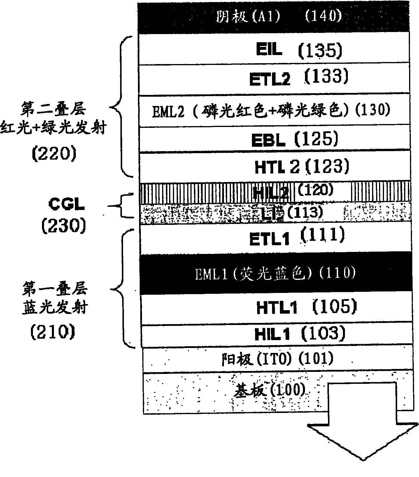
[0045] figure 1 is a sectional view illustrating an example of a white organic light emitting device according to the present invention.

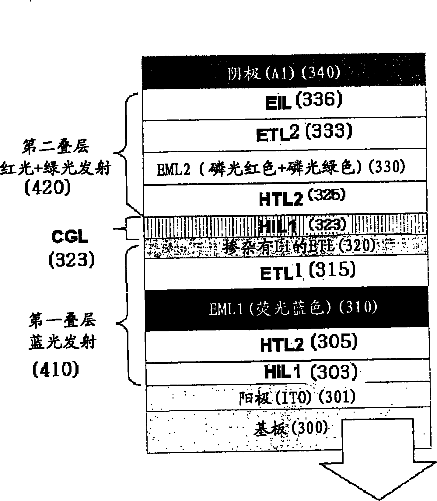
[0046] Such as figure 1As shown, the white organic light-emitting device according to the present invention includes an anode 101 and a cathode 140 facing each other on a substrate 100, a first stack 210 deposited between the anode 101 and the cathode 140, a charge generation layer (CGL) 230 and a second Two stacks 220 .

[0047] The charge generation layer 230 includes a stacked structure of the metal layer 113 and the second hole injection layer 120 from bottom to top.

[0048] The anode 101 is formed of a transparent electrode such as ITO (Indium Tin Oxide). ...


PUM


Abstract

Provided is a white organic light emitting device. The white organic light emitting device having a sack structure of blue fluorescence and red / green phosphorescence is disclosed, wherein efficiency of the blue fluorescence is improved to increase the lifespan of the white organic light emitting device, color quality is improved, and power consumption is reduced. The white organic light emitting device comprises an anode and a cathode facing each other on a substrate; a charge generation layer formed between the anode and the cathode; a first stack formed between the anode and the charge generation layer in a stack structure of a first hole transport layer, a first light emitting layer emitting blue, a first electron transport layer and an electron transport catalyst layer doped with metal; and a second stack formed between the charge generation layer and the cathode in a stack structure of a second hole transport layer, a second light emitting layer and a second electron transport layer. The second light emitting layer is doped with phosphor red and green dopants in one host, and the second hole transport layer has an energy level higher than a triplet exciton energy level of thesecond light emitting layer.

Description

technical field [0001] The present invention relates to an organic light emitting device, and more particularly, to a white organic light emitting device having a stacked structure of blue fluorescence and red / green phosphorescence, wherein the efficiency of blue fluorescence is improved to increase the lifetime of the white organic light emitting device , color quality is improved and power consumption is reduced. Background technique [0002] This application claims priority from Korean Patent Application No. 10-2009-92596 filed September 29, 2009, the contents of which are hereby incorporated by reference as if fully set forth herein. [0003] Recently, with the advent of the information age, the field of displays that visually display electrical information signals has been rapidly developed. In this regard, various flat panel display devices having excellent properties such as thin profile, light weight, and low power consumption are developed to quickly replace existi...

Claims


Application Information

Patent Timeline
Patent Type & Authority Applications(China)
IPC IPC(8): H01L51/50H01L51/54H10K99/00
CPCH01L2251/552H01L51/5036H10K59/32H10K50/131H10K50/125H10K2101/30H05B33/14H10K50/00
Inventor 皮性勋金昌五
Owner LG DISPLAY CO LTD
Learn More