Formation method for split gate storage device

A memory device and discrete gate technology, which is applied in semiconductor devices, semiconductor/solid-state device manufacturing, electrical components, etc., can solve the problems of large differences in electrical properties of memory cells with floating gate structure thickness differences, poor thickness uniformity, etc., and achieve overall thickness The effect of improving uniformity and ensuring consistency

Active Publication Date: 2011-05-04
SEMICON MFG INT (SHANGHAI) CORP +1
View PDF5 Cites 14 Cited by
  • Summary
  • Abstract
  • Description
  • Claims
  • Application Information

AI Technical Summary

Problems solved by technology

[0013] The above solution uses CMP to planarize the polysilicon material layer 222 to form a polysilicon layer with a floating gate structure. The thickness uniformity of the polysilicon layer with a floating gate structure obtained by using CMP

Method used


Image

  • Formation method for split gate storage device
  • Formation method for split gate storage device
  • Formation method for split gate storage device

Examples


Embodiment Construction

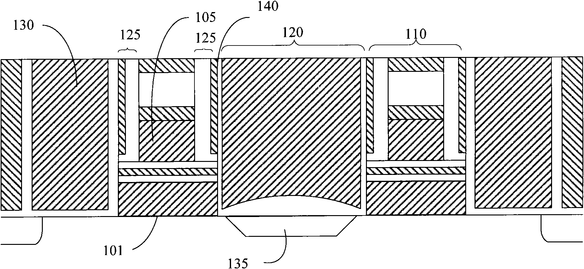
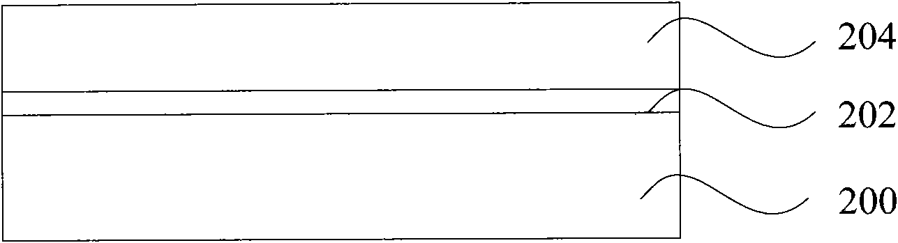
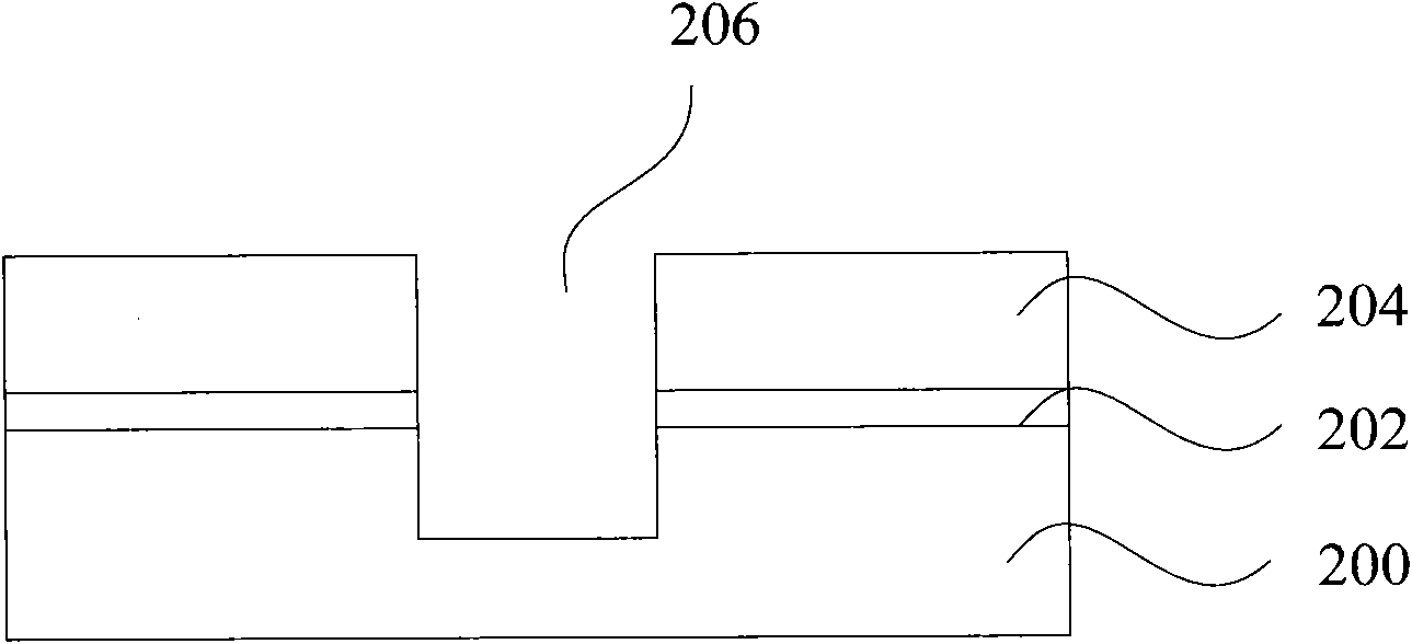
[0045] The embodiment of the present invention provides a method for forming a discrete gate storage device, which uses a self-aligned shallow trench isolation method to form a floating gate polysilicon layer, which solves the problem of poor thickness uniformity of the floating gate polysilicon layer obtained by a CMP process. In addition, since the thickness of the polysilicon layer of the floating gate is small, the tip of the floating gate can be formed by using the smile effect, which improves the erasing efficiency of the device.

[0046] In order to make the above objects, features and advantages of the present invention more comprehensible, specific implementations of the present invention will be described in detail below in conjunction with the accompanying drawings.

[0047] In the following description, specific details are set forth in order to provide a thorough understanding of the present invention. However, the present invention can be implemented in many other ...


PUM


Abstract

The invention discloses a formation method for a split gate storage device, which is composed of a semiconductor substrate, wherein the semiconductor substrate is successively provided with a gate dielectric layer, a floating gate polycrystalline silicon layer and a hard mask layer. The formation method comprises the following steps: performing trench isolation etching on the hard mask layer, floating gate polycrystalline silicon layer, gate dielectric layer and part of the semiconductor substrate to form isolated trenches; filling dielectric in the isolated trenches; and removing the hard mask layer. By adopting the self-alignment shallow slot isolation method to form the floating gate polycrystalline silicon layer, the thickness uniformity of the floating gate polycrystalline silicon layer is improved and the consistency of the erasing performance of storage units can be ensured.

Description

technical field [0001] The invention relates to the field of semiconductor technology, in particular to a method for forming a discrete gate storage device. Background technique [0002] With the development of the semiconductor industry, due to the wide application of memory devices, their output accounts for a considerable proportion of integrated circuit products. Among storage devices, the development of flash memory (flash memory for short) is particularly rapid in recent years. The main feature of flash memory is that it can keep stored information for a long time without power on; and it has the advantages of high integration, fast access speed, easy erasing and rewriting, etc. Therefore, flash memory has been widely used in many fields such as computers and automation control. widely used. [0003] The standard physical structure of flash memory is called a memory cell (bit). The structure of flash memory is different from that of conventional MOS transistors. Usu...

Claims


Application Information

Patent Timeline
IPC IPC(8): H01L21/8247H01L21/28H01L21/762
Inventor 李勇刘艳周儒领黄淇生
Owner SEMICON MFG INT (SHANGHAI) CORP
Why Eureka
Try Eureka