

Three-dimensional integrated structure and production methods thereof
A three-dimensional integration and production method technology, applied in microstructure technology, microstructure devices, manufacturing microstructure devices, etc., can solve problems such as the impact of MEMS device integrated circuit IC performance, improve the performance of MEMS devices, solve compatibility problems, Guaranteed high density effect
- Summary
- Abstract
- Description
- Claims
- Application Information
AI Technical Summary
Problems solved by technology
Method used
Image

Examples
Embodiment 1
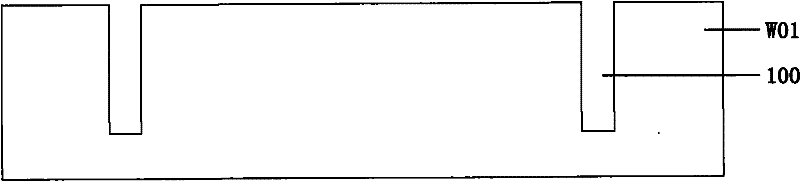
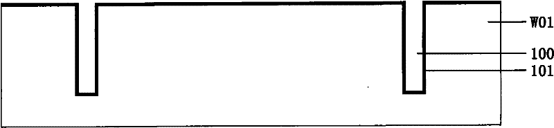
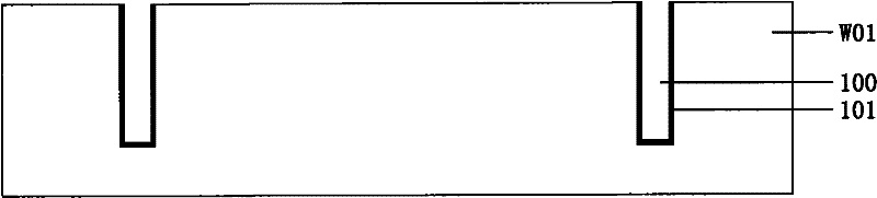
[0056] Step 1-1, making TSV deep holes 100 on the first silicon wafer W01, performing oxidation treatment, and then removing the silicon dioxide on the surface of the silicon wafer W01, so that the side walls of the TSV deep holes 100 are covered by an oxide layer 101 (such as Figure 1-1 to Figure 1-3 shown). The etching of the TSV deep hole 100 may adopt etching technologies such as RIE, DRIE, etc., and may also adopt technologies such as laser drilling and mechanical drilling. Oxidation can use low pressure chemical vapor deposition (LPCVD), plasma enhanced chemical vapor deposition (PECVD), dry oxygen, or wet oxygen and other techniques.
[0057] Step 1-2, etching the recessed region 210 on the second silicon wafer W02, and etching the TSV deep hole 200; performing oxidation treatment, and then removing the silicon dioxide on the surface of the silicon wafer W02, so that the side wall of the TSV deep hole 200 Obtain oxide layer 201 coverage (eg Figure 2-1 to Figure 2-4 s...
Embodiment 2
[0068] Step 1, taking the first silicon wafer and the second silicon wafer for use. Etching the recessed region 210 on the second silicon wafer W02, such as Figure 7 shown. The etching of the recessed region 210 may adopt etching techniques such as RIE, DRIE, or other techniques.
[0069] Step 2. Bond the surface where the recessed region 210 is located to the first silicon wafer, then make TSV via holes, and perform insulation treatment on the side walls of the TSV, such as Figure 8-1 to Figure 8-4 shown. Silicon-silicon fusion bonding may be used for bonding.
[0070] This step may include a step of thinning the bonded wafer pair. Thinning technology can use chemical mechanical polishing (CMP) technology, or wet etching technology such as TMAH and KOH.
[0071] TSV through holes can be made by RIE, DRIE etching technology, laser drilling, mechanical drilling and other technologies.
[0072] The insulation of the TSV sidewalls can be achieved by depositing silicon dio...
PUM
 Abstract
Description
Claims
Application Information