Transverse high-voltage MOS device and manufacturing method thereof

A MOS device and lateral high voltage technology, which is applied in semiconductor/solid-state device manufacturing, semiconductor devices, electrical components, etc., can solve the problems of device damage, reduced device performance, high dependence, etc., achieve good process stability, reduce surface electric field, The effect of improving the withstand voltage performance

Active Publication Date: 2011-05-11
SHANGHAI HUAHONG GRACE SEMICON MFG CORP
View PDF0 Cites 6 Cited by
  • Summary
  • Abstract
  • Description
  • Claims
  • Application Information

AI Technical Summary

Problems solved by technology

[0003] Existing lateral high-voltage MOS devices will generate excessively high surface electric fields, which limits the improvement of their withstand voltage performance. Under high-voltage and high-current operating conditions, gate oxide layer breakdown is prone to occur, causing device damage and seriously affecting device reliability. sex
The commonly used internal field limiting ring is not suitable for devices with a smaller size. For small-sized high-voltage tubes that do not require particularly high withstand voltages, it will cause high on-resistance and reduce device performance.
The commonly used Reduced surface field (RESURF) technology is too dependent on process conditions such as epitaxial layer thickness and concentration, which is not conducive to the use of platforms containing multiple types of devices

Method used


Image

  • Transverse high-voltage MOS device and manufacturing method thereof
  • Transverse high-voltage MOS device and manufacturing method thereof
  • Transverse high-voltage MOS device and manufacturing method thereof

Examples


Embodiment Construction

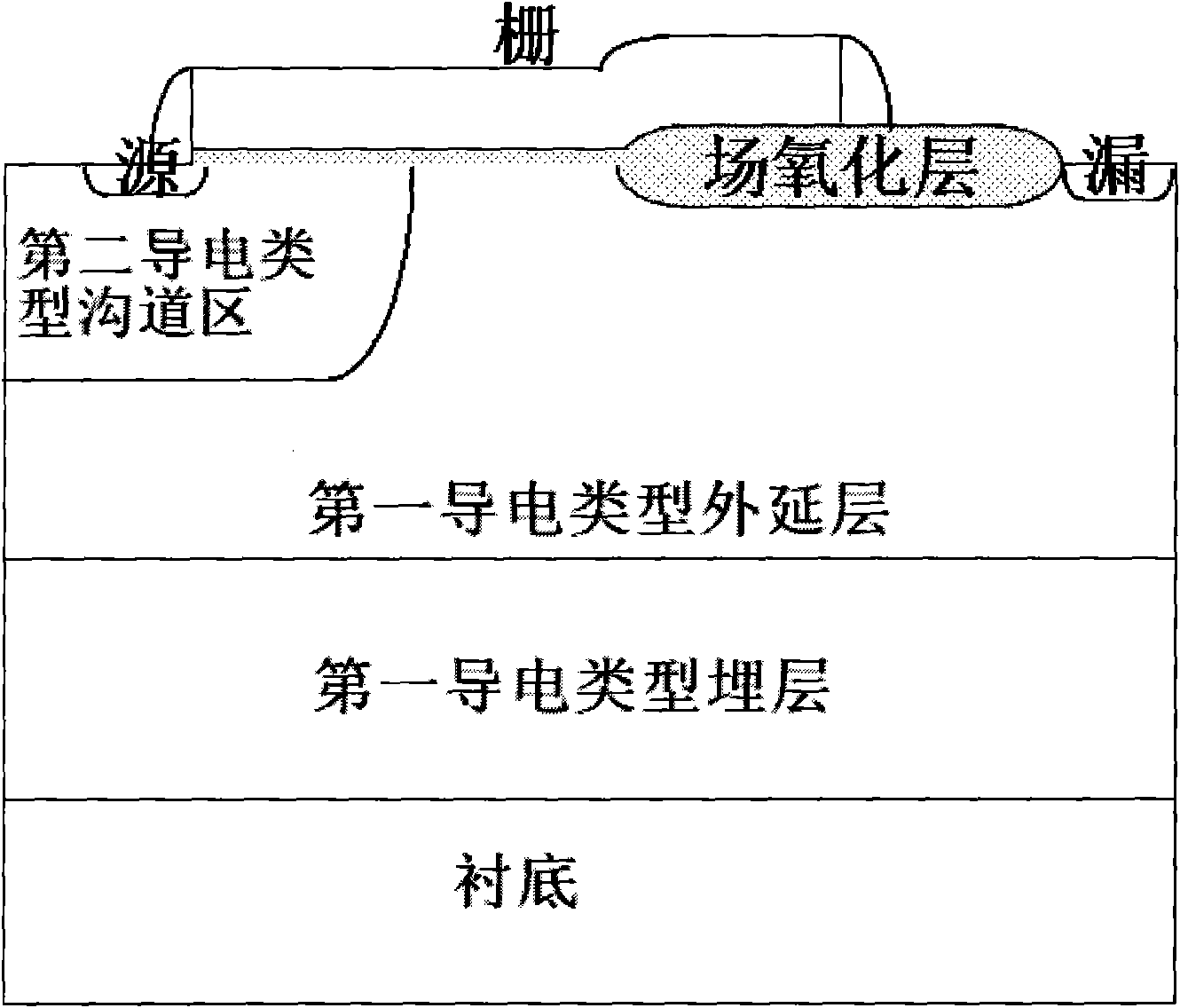
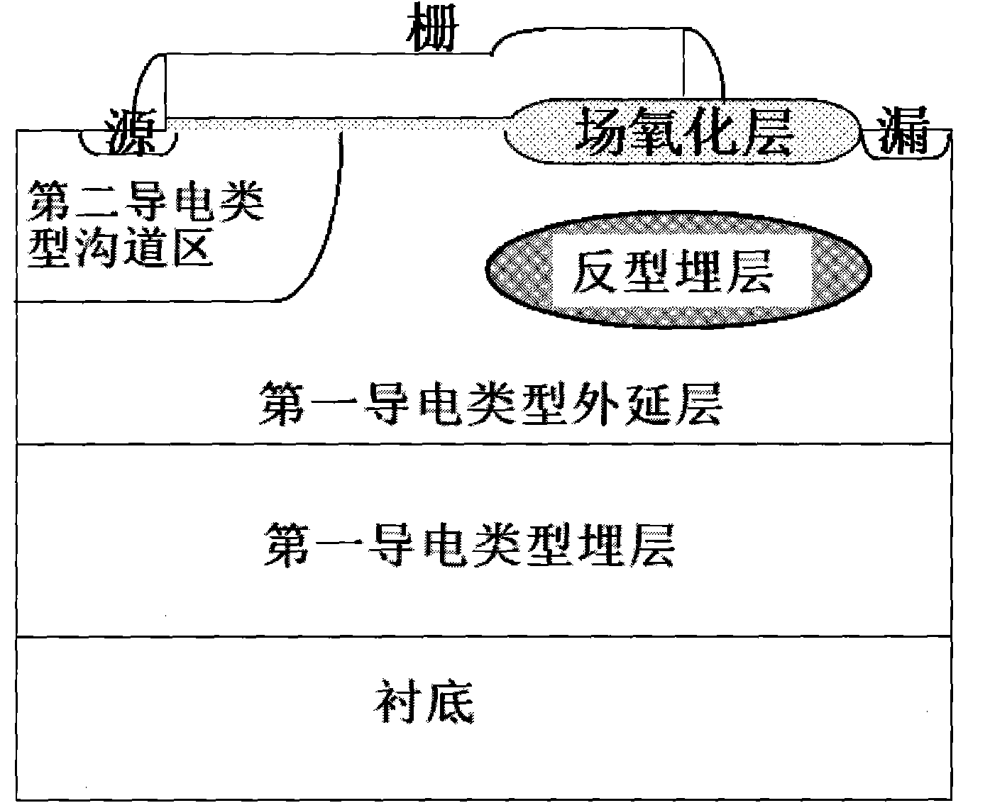
[0023] Such as figure 2 Shown is a schematic structural view of the lateral high voltage MOS device of the present invention. The method includes: forming a first conductivity type buried layer on a silicon substrate, and forming a first conductivity type epitaxial layer on the first conductivity type buried layer; forming a second conductivity type epitaxial layer in the first conductivity type epitaxial layer. type channel region, forming a heavily doped first conductivity type source region in the second conductivity type channel region; forming a heavily doped first conductivity type drain region in the first conductivity type epitaxial layer; The epitaxial layer of the first conductivity type between the channel region and the drain region is used as a drift region of the device; a field oxide layer is formed on the drift region and is connected to the drain region; a gate oxide layer is formed on the channel region, and the gate The oxide layer covers the entire channe...


PUM


Abstract

The invention discloses a transverse high-voltage metal oxide semiconductor (MOS) device, which is formed by burying an inversion buried layer into a drifting region of the device. The invention also discloses a method for manufacturing the transverse high-voltage MOS device, which comprises the following steps of: forming a first conduction type buried layer, a first conduction type epitaxial layer and a sacrifice oxide layer on a silicon substrate, and determining an implantation position of the inversion buried layer in the drifting region by adopting a photoetching process; performing second conduction type foreign ion implantation by taking photoresist as a mask to form an inversion impurity region; manufacturing a field oxide layer, and activating and boosting inversion impurities simultaneously in the thermal process of growing the field oxide layer to form the shallow inversion buried layer in the drifting region; and forming a channel region, a source oxide layer, a drain oxide layer, a gate oxide layer and a gate. Electric-field distribution in the drifting region can be changed, a surface electric field of a device can be reduced and withstand voltage performance and reliability can be improved.

Description

technical field [0001] The invention relates to the field of manufacturing semiconductor integrated circuits, in particular to a lateral high-voltage MOS device, and also relates to a method for manufacturing the lateral high-voltage MOS device. Background technique [0002] Lateral high-voltage MOS devices have high withstand voltage and are easy to integrate, and are widely used in high-voltage integrated circuits and power integrated circuits. Such as figure 1 As shown, it is an existing lateral high-voltage MOS device, and the device structure is: a buried layer of the first conductivity type is formed on a silicon substrate, and an epitaxial layer of the first conductivity type is formed on the buried layer of the first conductivity type; A channel region of the second conductivity type is formed in the epitaxial layer of the first conductivity type, and a heavily doped source region of the first conductivity type is formed in the channel region of the second conductiv...

Claims


Application Information

Patent Timeline
Patent Type & Authority Applications(China)
IPC IPC(8): H01L29/78H01L29/36H01L21/336H01L21/265
Inventor 钱文生韩峰
Owner SHANGHAI HUAHONG GRACE SEMICON MFG CORP
Why Eureka
Try Eureka