Computer based on programmable hardware computing platform

A computing platform and computer technology, applied in electronic science and fields, to achieve the effect of improving parallelism and computing efficiency, avoiding clock domain convergence problems, and reducing work performance

Inactive Publication Date: 2012-05-23
UNIV OF SCI & TECH OF CHINA
View PDF0 Cites 0 Cited by
  • Summary
  • Abstract
  • Description
  • Claims
  • Application Information

AI Technical Summary

Problems solved by technology

[0007] In order to solve the above-mentioned technical problems, the object of the present invention is to provide a computer based on a programmable hardware computing platform to solve the problem that it is difficult for a dedicated computing platform in the prior art to improve the parallelism and computing efficiency of operations by increasing the area of ​​the chip. problems, and at the same time realize the softwareization of computer hardware design

Method used


Image

  • Computer based on programmable hardware computing platform
  • Computer based on programmable hardware computing platform
  • Computer based on programmable hardware computing platform

Examples


Embodiment 1

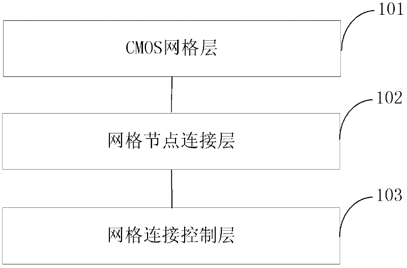
[0048] see figure 1 As shown, it is a schematic structural diagram of a computer based on a programmable hardware computing platform provided in this embodiment, which specifically includes:

[0049] The CMOS grid layer 101 is composed of multiple grid units tiled. Each grid unit includes multiple MOS transistor pairs and multiple connection nodes. Adjacent grid units are connected to each other through shared connection nodes. Each connection The nodes are respectively connected to multiple MOS tube pairs in the grid unit where they are located;

[0050] The grid node connection layer 102 includes a plurality of grid nodes, and each grid node is connected to a connection node in the grid unit, including a plurality of shielding switches and node state switches, and the shielding switch controls the working state of the MOS tube pair, and the node The state switch is used to control the connection state between the MOS tube pairs;

[0051] The grid connection control layer 1...

Embodiment 2

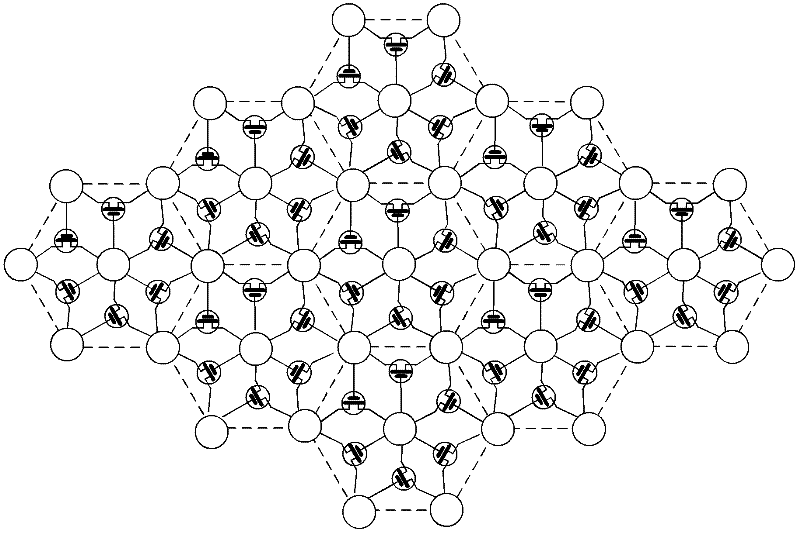
[0059] This embodiment provides a specific structure of the CMOS grid layer described in Embodiment 1, see Figure 2a Shown is a schematic diagram of a specific structure of a CMOS grid layer in a computer based on a programmable hardware computing platform.

[0060] Wherein the grid unit can be a regular hexagonal structure, and each grid unit includes 6 MOS transistor pairs and multiple connection nodes; each MOS transistor pair includes an NMOS transistor and a PMOS transistor with the same direction; each connection The node includes 12 connection channels, which are respectively connected to 6 MOS tube pairs. As shown in FIG. 2 , the MOS transistors graphically represent pairs of MOS transistors that are composed of NMOS transistors and PMOS transistors in the same direction, and all circles in the figure represent connection nodes. Due to the symmetry of the drain and source of the MOS transistor, the position of the drain and source of each NMOS transistor and PMOS tra...

Embodiment 3

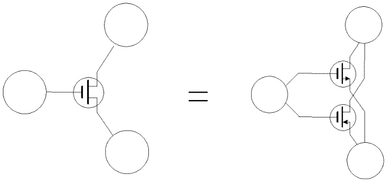
[0074] This embodiment provides a specific structure of the grid node described in Embodiment 1, see Figure 7 As shown, it is a schematic diagram of the serial number of a connection node and the pair of MOS transistors it is connected to. The MOS transistor graphic represents a pair of MOS transistors composed of NMOS transistors and PMOS transistors with the same direction. The circle shown in the graph represents Connect the nodes. see Figure 8 As shown, it is a schematic diagram of the structure of the grid node:

[0075] Wherein: the pins of the two NMOS transistors on the diagonal of each connection node are connected to each other; the pins of the two PMOS transistors are connected to each other.

[0076] Each grid node may include 6 shielding switches, and the gates of the 6 MOS transistors in the 3 MOS transistor pairs are respectively connected to the corresponding shielding switches through the connection nodes;

[0077] The shielding switch is used to separate...


PUM


Abstract

The invention discloses a computer based on a programmable hardware computing platform, comprising a CMOS (Complementary Metal Oxide Semiconductor) grid layer, a grid node connection layer and a grid connection control layer, wherein the CMOS grid layer is formed by tiling a plurality of grid units, and each grid unit comprises a plurality of MOS pipe pairs and a plurality of connection nodes; the grid node connection layer comprises a plurality of grid nodes, and each grid node comprises a plurality of shielding switches and a node state switch. The computer provided by the invention is reconfigurable, the connection node is used for replacing complex routing in the traditional FPGA (Field Programmable Gate Array), and all signal connection and function realizations happen on the connection node; and the platform structure has integral topology consistency so as to support the operations of copying, moving and linking a hardware module, thus realizing the hardware processing to software. In the platform, the design of an asynchronous circuit does not need a global clock and avoids the problem of clock domain astringency due to computer chip area and routing length so as to improve the operation parallelism degree and the operation efficiency of the computer chip.

Description

Technical field: [0001] The invention relates to the field of electronic science and technology, in particular to a computer based on a programmable hardware computing platform. Background technique: [0002] Since the birth of the first computer in 1946, the development of computer science and technology is changing the way of life of human beings and leading a new revolution in human society. With the development of the semiconductor process level and the improvement and improvement of the processor architecture, the current computer structure is sufficient to meet most of human needs. But in some special application fields, this kind of general computer structure shows certain deficiencies. For example, for some application fields that require a large number of cyclic operations (such as repeated iterative calculations common to finite element methods), the computing power of existing computers is insufficient. At the same time, in some stream processing applications wit...

Claims


Application Information

Patent Timeline
Patent Type & Authority Patents(China)
IPC IPC(8): G06F15/76
Inventor 杨俊峰宋克柱曹平
Owner UNIV OF SCI & TECH OF CHINA
Why Eureka
Try Eureka