Single event resistance latch structure based on state saving mechanism

An anti-single event, state preservation technology, applied in the direction of pulse generation, electrical components, reliability improvement and modification, etc., can solve the problems of increasing system timing overhead, achieve small area and power consumption, simple circuit structure, and reduce occupied area Effect

Active Publication Date: 2011-05-18
58TH RES INST OF CETC
View PDF4 Cites 14 Cited by
  • Summary
  • Abstract
  • Description
  • Claims
  • Application Information

AI Technical Summary

Problems solved by technology

The limitation of this method is that using a separate delay filter will increase the overhead of system timing
The structure of triple-mode redundancy plus majority voter can completely eliminate the single event effect on the circuit, but it will bring up to 3.5 times the additional overhead in terms of area and power consumption

Method used


Image

  • Single event resistance latch structure based on state saving mechanism
  • Single event resistance latch structure based on state saving mechanism
  • Single event resistance latch structure based on state saving mechanism

Examples


Embodiment Construction

[0018] The present invention will be further described below in conjunction with specific drawings and embodiments.

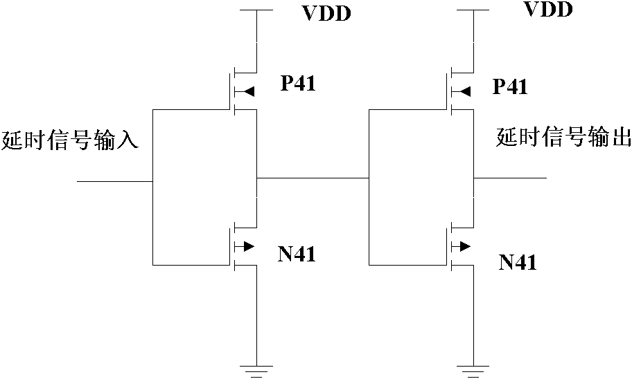
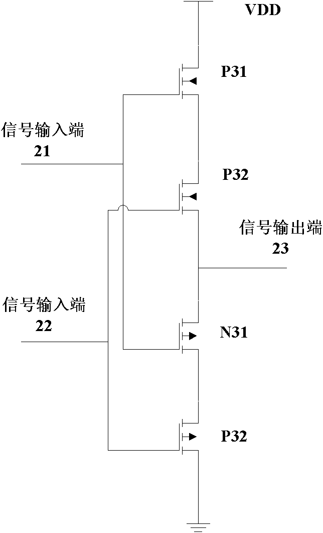
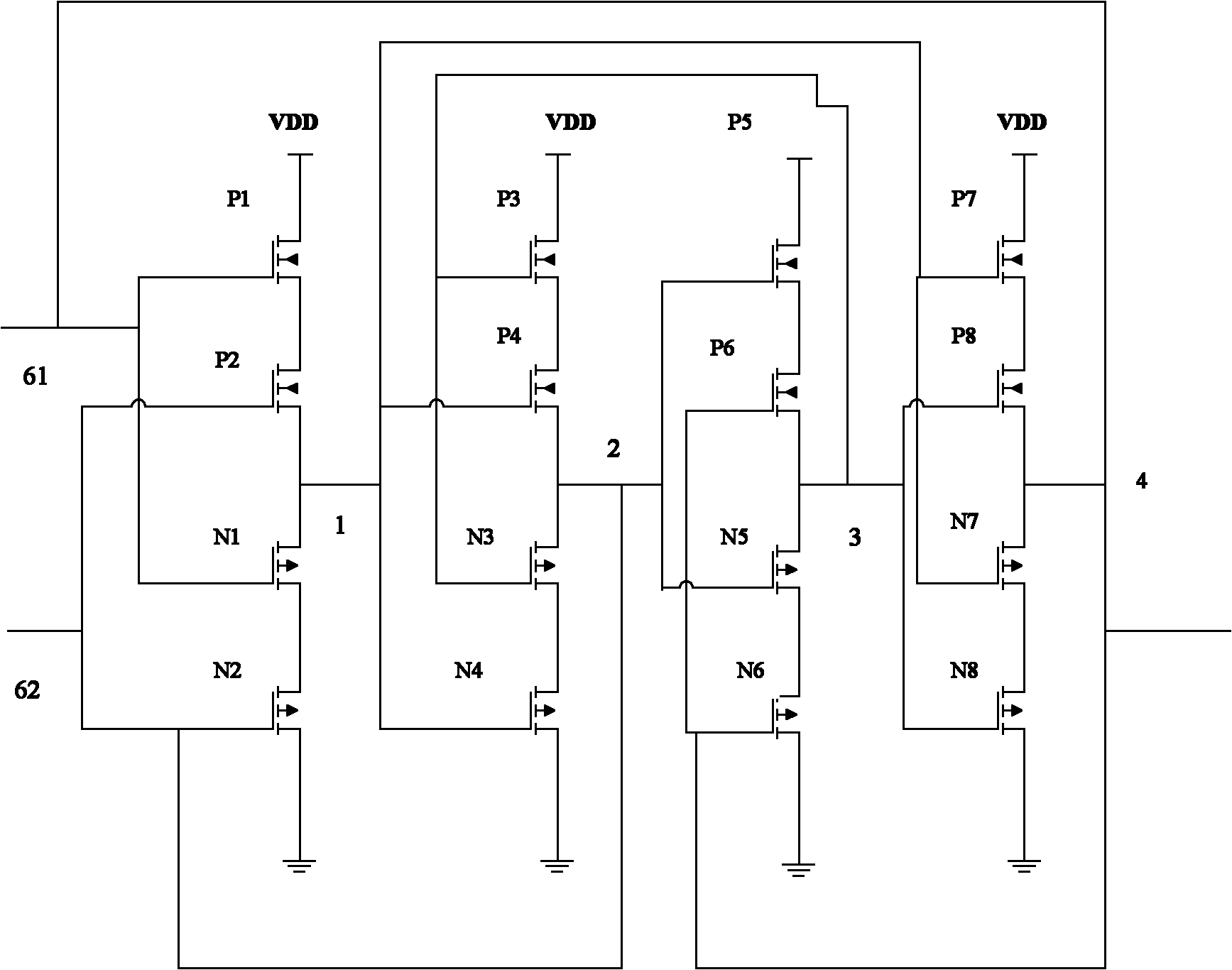
[0019] Such as Figure 1~Figure 4 As shown: the present invention includes a signal delay circuit, an anti-single event latch circuit, a first node 1, a second node 2, a third node 3, a fourth node 4, a control signal input terminal 5, a data input terminal 6, a data The output terminal 7 , the first latch circuit input terminal 61 and the second latch circuit input terminal 62 .

[0020] figure 1 Schematic diagram of the signal delay circuit. figure 1 In , only one set of inverter delay circuits in the signal delay circuit is shown. Such as figure 1 As shown: the inverter delay circuit includes two inverters; the inverter includes a MOS transistor P41 and a MOS transistor N41, the source terminal of the MOS transistor P41 is connected to the power supply VDD, and the drain terminal of the MOS transistor P41 is connected to the power supply VDD. The drain ...


PUM


Abstract

The invention relates to a single event resistance latch structure based on a state saving mechanism, comprising a signal time delay circuit and a single event resistance latch circuit, wherein the delay time of the time delay circuit is more than the maximum pulse width generated by the transient disturbance of a single event; the single event resistance latch circuit simultaneously receives and compares an external input signal and an external input time delay signal of the external input signal, which is output by the signal time delay circuit; when the external input signal and the external input time delay signal are same, the single event resistance latch circuit outputs and latches a corresponding state signal according to the state of the external input signal; and when the external input signal and the external input time delay signal are different, the single event resistance latch circuit outputs a state signal latched by the single event resistance latch circuit on the previous moment. The single event resistance latch structure provided by the invention improves the restoring speed after a circuit is disturbed by the single event, can prevent SEU (Single Event Upset) effect and SET (Single Event Transient) effect from disturbing the circuit, has simple circuit structure, reduces occupation area, lowers power consumption and improves system reliability.

Description

technical field [0001] The present invention relates to an anti-single event latch structure, especially an anti-single event latch structure based on a state preservation mechanism, specifically a latch structure capable of resisting single event flipping and preventing single event disturbance . Background technique [0002] When electronic devices work in space, they will be hit by high-energy protons, high-energy neutrons and heavy particles in the universe. The impact itself, as well as the secondary particles produced by the impact, ionize electron-hole pairs on the bulk silicon; when the amount of charge accumulated by the ionization reaches a certain magnitude, it will disturb the state of the circuit. Such as: bit flips in memory cells, transient pulses in combinational logic, etc. These effects are often called single event effects. Single event effects can be divided into: single event latch-up (SEL), single event upset (SEU), single event transient disturbance...

Claims


Application Information

Patent Timeline
Patent Type & Authority Applications(China)
IPC IPC(8): H03K19/003H03K3/013
Inventor 周昕杰薛忠杰王栋罗静徐睿周毅
Owner 58TH RES INST OF CETC
Why Eureka
Try Eureka