Reinforced linear gradient doped GaAs planar Gunn diode and manufacturing method thereof

A Gunn diode and gradient doping technology, applied in electrical components, bulk negative resistance effect devices, circuits, etc., can solve the problem of the weakening of RF output power and conversion efficiency, the reduction of the effective length of the N-type active region, and the inability to output oscillation. Frequency tuning and other issues to achieve the effect of increasing RF output power and conversion efficiency, facilitating heat conduction and improving thermal stability

Inactive Publication Date: 2011-05-25
INST OF MICROELECTRONICS CHINESE ACAD OF SCI
View PDF0 Cites 3 Cited by
  • Summary
  • Abstract
  • Description
  • Claims
  • Application Information

AI Technical Summary

Problems solved by technology

The double-terminal Gunn diode with this doping structure, in the millimeter wave and submillimeter wave frequency range, the effective length of the N-type active region is reduced, and the RF output power and conversion efficiency are weakened; the Gunn diode with this doping structure cannot Use DC voltage to directly tune the output oscillation frequency; double-ended Gunn diodes are not conducive to monolithic integration, resulting in the need for a large number of device carriers, external bias circuits, and metal waveguides in the system.

Method used


Image

  • Reinforced linear gradient doped GaAs planar Gunn diode and manufacturing method thereof
  • Reinforced linear gradient doped GaAs planar Gunn diode and manufacturing method thereof
  • Reinforced linear gradient doped GaAs planar Gunn diode and manufacturing method thereof

Examples


Embodiment Construction

[0040] In order to make the object, technical solution and advantages of the present invention clearer, the present invention will be described in further detail below in conjunction with specific embodiments and with reference to the accompanying drawings.

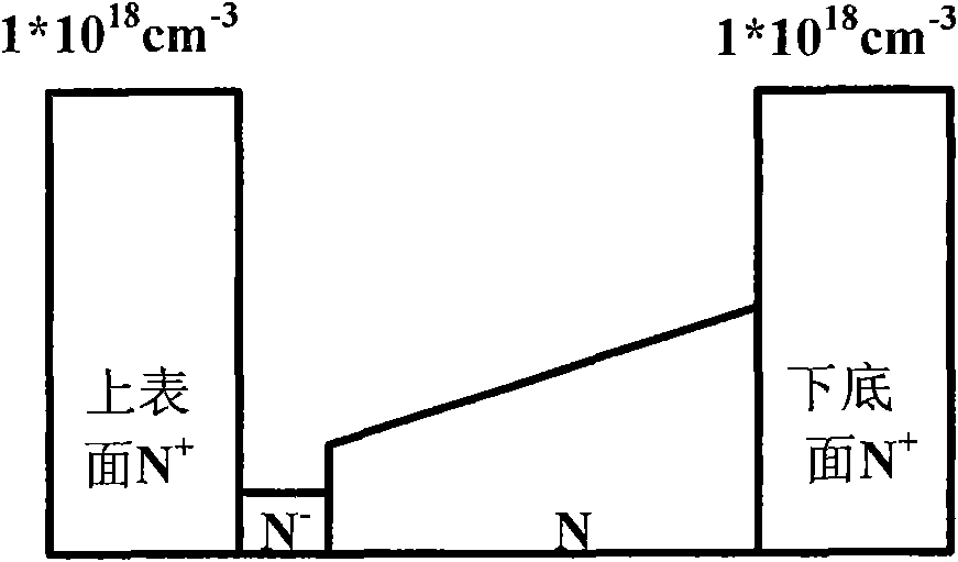
[0041] like figure 1 as shown, figure 1 The carrier concentration distribution diagram of the enhanced linear gradient doping GaAs planar Gunn diode material structure provided by the present invention.

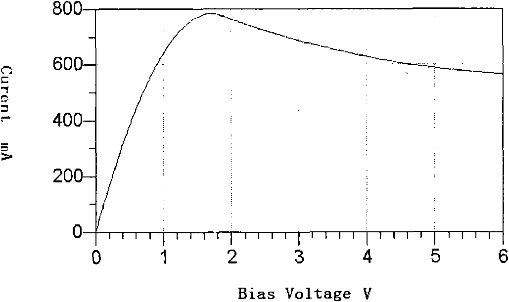
[0042] like figure 2 as shown, figure 2 The DC simulation result of the enhanced linear gradient doping GaAs planar Gunn diode material structure provided by the present invention. It can be seen from the figure that when the applied DC voltage is greater than 1.8 volts, the Gunn diode exhibits negative differential resistance characteristics.

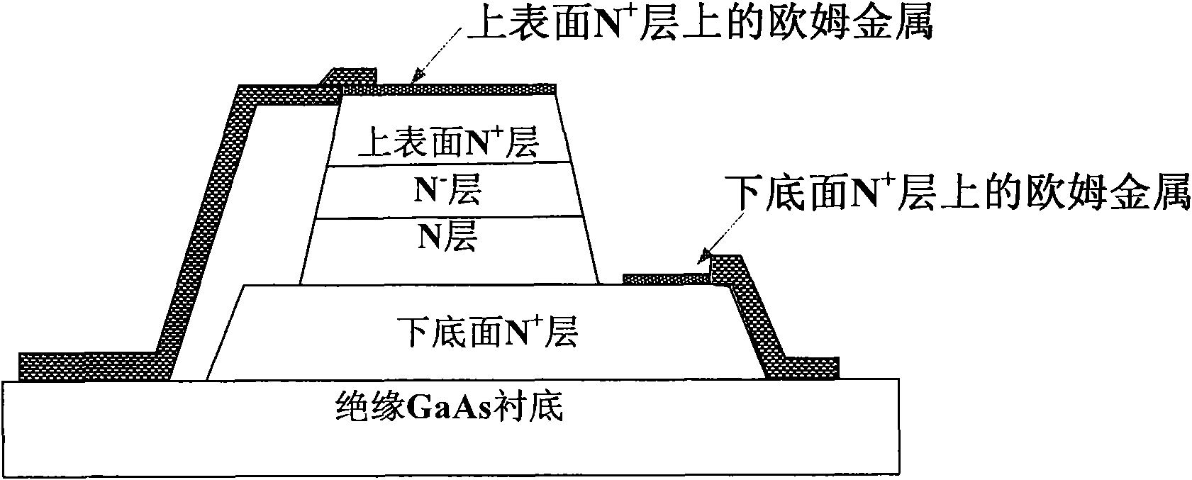
[0043] like image 3 as shown, image 3 A cross-sectional view of an enhanced linear gradient doped GaAs planar Gunn diode provided by the present invention. The cross-s...


PUM


Abstract

The invention discloses a reinforced linear gradient doped GaAs planar Gunn diode, which comprises a semiconductor insulated substrate, a high doped bottom N+ layer, a linear gradient doped N layer, an N- layer, a high doped upper surface N+ layer, a table top structure, an upper electrode and a lower electrode, wherein the semiconductor insulated substrate is used for supporting the whole GaAs planar Gunn diode; the high doped bottom N+ layer is epitaxially grown on the semiconductor insulated substrate; the linear gradient doped N layer is continuously epitaxially grown on the bottom N+ layer; the N- layer is epitaxially grown on the linear gradient doped N layer; the high doped upper surface N+ layer is epitaxially grown on the N- layer; the table top structure is formed on the bottom N+ layer and the upper surface N+ layer by two processes of digging and isolating; the upper electrode of ohmic contact is formed by evaporating metal on the upper surface N+ layer; and the lower electrode of ohmic contact is formed by evaporating metal on the bottom N+ layer. The invention discloses a manufacturing method for the reinforced linear gradient doped GaAs planar Gunn diode at the same time. By using the diode, the working frequency of an oscillating circuit in a millimeter wave or sub millimeter wave range is improved, and the conversion efficiency of direct current-to-radio frequency signals is enhanced.

Description

technical field [0001] The invention relates to the technical field of diodes in microwave devices, in particular to an enhanced linear gradient doped GaAs planar Gunn diode and a manufacturing method thereof. Background technique [0002] Oscillators based on nonlinear devices such as Gunn diodes are often used as high-frequency local oscillator sources. Gunn diodes are active nonlinear devices of millimeter-wave oscillators. Due to the continuous development of high-quality semiconductor material manufacturing, processing technology and assembly technologies, the devices show excellent performance. At the same time, the preparation process of Gunn diodes is simple and the structure is flexible, so they are not only used as local oscillator sources for various receiver mixers, but also can be used as small and medium power signal sources in radar, communication, space technology, etc., and are currently the most widely used. semiconductor oscillator. [0003] Traditional ...

Claims


Application Information

Patent Timeline
Patent Type & Authority Applications(China)
IPC IPC(8): H01L47/02
Inventor 黄杰杨浩董军荣吴茹菲张海英
Owner INST OF MICROELECTRONICS CHINESE ACAD OF SCI
Why Eureka
Try Eureka