

Linear gradient doped GaAs planar gunn diode and manufacturing method thereof
A Gunn diode, gradient doping technology, applied in electrical components, body negative resistance effect devices, circuits, etc., can solve the problems of unfavorable monolithic integration, failure to output oscillation frequency tuning, etc., to achieve easy monolithic integration and improve conversion The effect of efficiency and flexible structure
- Summary
- Abstract
- Description
- Claims
- Application Information
AI Technical Summary
Problems solved by technology
Method used
Image

Examples
Embodiment Construction
[0040] In order to make the object, technical solution and advantages of the present invention clearer, the present invention will be described in further detail below in conjunction with specific embodiments and with reference to the accompanying drawings.
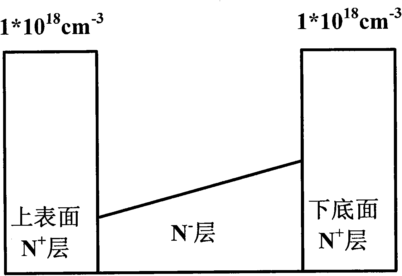
[0041] Such as figure 1 as shown, figure 1 The linear gradient doping carrier concentration distribution diagram of the GaAs planar Gunn diode provided by the present invention.
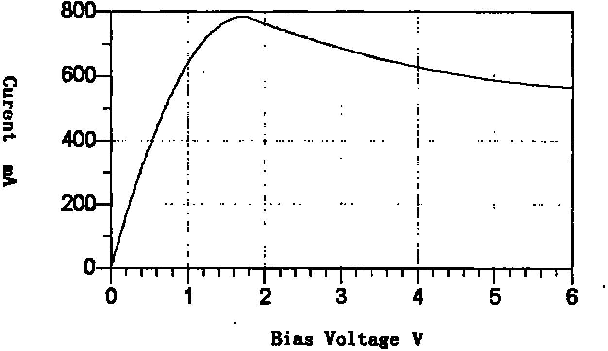
[0042] Such as figure 2 as shown, figure 2 The DC simulation results of the GaAs planar Gunn diode material structure provided by the present invention are linear gradient doping. It can be seen from the figure that when the applied DC voltage is greater than 1.8 volts, the Gunn diode exhibits negative resistance characteristics.
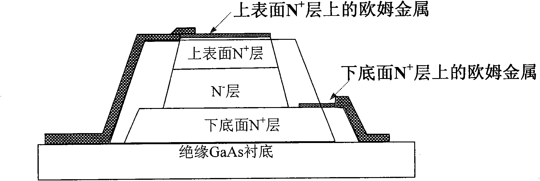
[0043] Such as image 3 as shown, image 3 A cross-sectional view of a GaAs planar Gunn diode with linear gradient doping provided by the present invention. The cross-sectional view is a cross-sectional view ...
PUM
 Abstract
Description
Claims
Application Information