Method for realizing micronano all-optical color

A color, micro-nano technology, applied in the field of nanophotonics, can solve the problems of not being able to use red light, not being able to realize full-color display, complex lithography technology of photonic crystals, etc., and achieve the effect of simple assembly

Inactive Publication Date: 2011-06-01
SUN YAT SEN UNIV
View PDF2 Cites 1 Cited by
  • Summary
  • Abstract
  • Description
  • Claims
  • Application Information

AI Technical Summary

Problems solved by technology

However, due to the limitation of the photonic crystal band gap, this method cannot be used for red light, so the full-color display based on the mixture of red, green and blue primary colors cannot be realized....

Method used


Image

  • Method for realizing micronano all-optical color
  • Method for realizing micronano all-optical color
  • Method for realizing micronano all-optical color

Examples


Embodiment 1

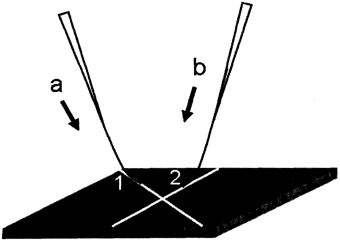
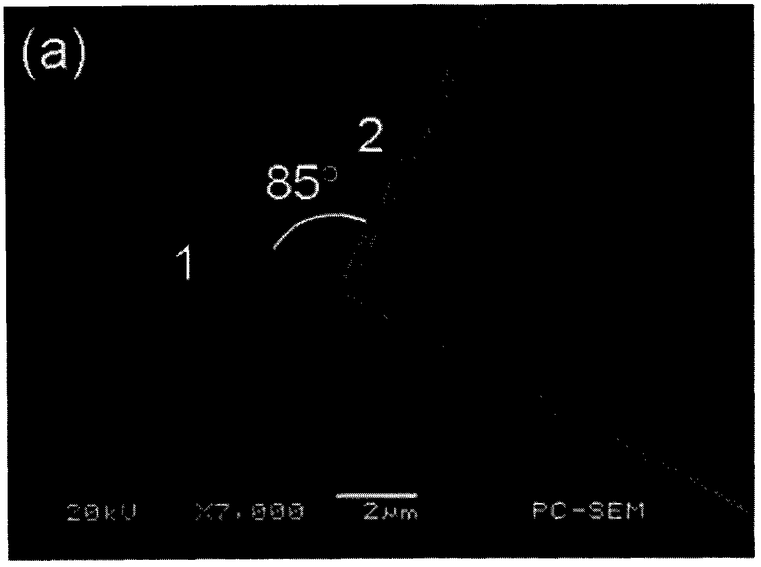
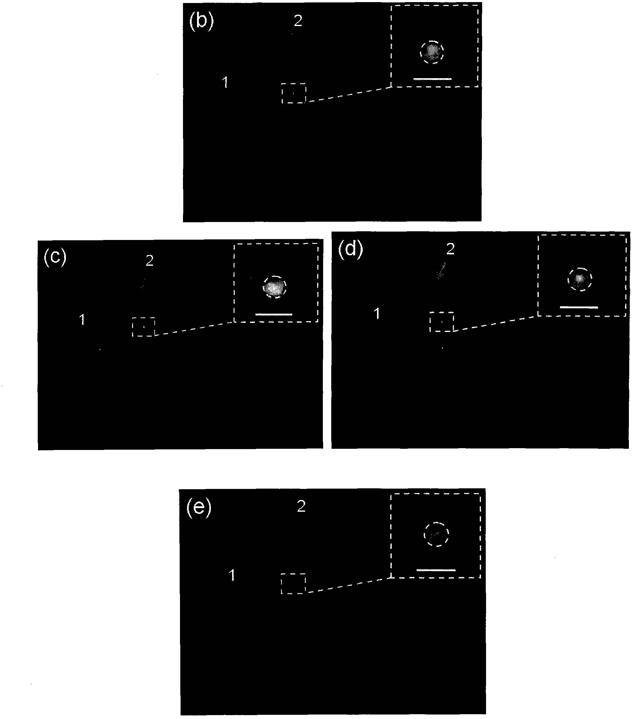
[0027] Nanowires 1 and 2 with diameters of 457nm and 486nm respectively constitute a cross junction, and the crossing angle of nanowires 1 and 2 is 85°. figure 2 In b, the optical power ratio of red light (wavelength, 650 nm) and green light (wavelength, 532 nm) coupled into nanowires 1 and 2 is about 6:10. The light spot formed at the cross junction is yellow-green, the radius of the light spot is 301 nm, and the chromaticity coordinates of the light spot are (0.27, 0.70). figure 2 In c-e, the optical power ratios of red light and green light coupled into nanowires 1 and 2 are 26:9, 27:4, and 32:2, respectively, and the colors of the light spots at the intersection junctions are green-yellow, orange, and red-orange, respectively , the corresponding spot radii are 303nm, 306nm, 310nm, and the corresponding chromaticity coordinates are (0.45, 0.54), (0.56, 0.43), (0.64, 0.35). (Such as figure 1 , figure 2 shown)

Embodiment 2

[0029] The diameters of nanowires 1, 2, and 3 are 558nm, 598nm, and 598nm respectively, nanowires 1 and 2 are perpendicular, and the crossing angle between wires 2 and 3 is 50°. Couple the red light, green light and blue light (wavelength, 473nm) with a power ratio of 50:13:10 to the cross junction, the white spot formed at the cross junction, the radius of the spot is 818nm, and the chromaticity coordinates of the spot are (0.41, 0.35 ), the corresponding correlated color temperature is 3026K. (Such as image 3 , Figure 4 shown)

Embodiment 3

[0031] Figure 5 a is a schematic diagram of a 2 × 6 nanowire array structure. Figure 5 In b, the diameters of nanowires 1-8 are 622nm, 638nm, 734nm, 765nm, 574nm, 613nm, 629nm, and 670nm, respectively, and the optical power ratio of the green light coupled to nanowires 1 and 2 is 19:20. The power ratio of the red light on lines 3-8 is 72:43:39:40:49:50, and the spot colors at the intersection A-L are yellow-orange, light yellow-green, yellow-green, yellow-green, red-orange, red-orange, Yellow-green, light yellow-green, light yellow-green, yellow-orange, orange, red-orange. The degree coordinates are (0.51, 0.48), (0.37, 0.60), (0.40, 0.58), (0.45, 0.54), (0.59, 0.39), (0.61, 0.38), (0.45, 0.53), (0.36, 0.61 ), (0.36, 0.62), (0.51, 0.49), (0.58, 0.41), (0.60, 0.39).


PUM

PropertyMeasurementUnit
Diameteraaaaaaaaaa

Abstract

The invention belongs to the field of nanophotonics, and discloses a method for realizing a micronano all-optical color. The method comprises the following steps of: arranging two or three nanowires on a glass substrate in turn to form a cross knot; coupling red light, green light or blue light into the nanowires through optical fibers connected with the nanowires respectively; and synthesizing colored light spots in various colors at the cross knot. In the method, an electric driver or a color filter is not needed; and the method has the advantages of easiness in fabrication and the like.

Description

technical field [0001] The invention belongs to the field of nanophotonics, and relates to a method for realizing micro-nano plenoptic color. Background technique [0002] Nanophotonics is an exciting emerging high-tech frontier discipline in the field of nanotechnology. Nanowires are an important research direction in nanophotonics and are the product of the combination of modern science and technology. Micro-nano plenoptic color display is another promising potential application field of nanowires besides micro-nano sensing. [0003] In recent years, color displays based on nanomaterials have received extensive attention, including: quantum dots, nanowires, organic light-emitting diodes, photonic crystals, resonant cavities, etc. But both are limited to electrically driven emission. In order to avoid the use of electric drive, people proposed a method based on two-dimensional photonic crystal slabs to realize micro-nano color display by introducing line-defect waveguides...

Claims


Application Information

Patent Timeline
IPC IPC(8): G02B6/24B81C1/00B82Y20/00
Inventor 李宝军余华清廖东威
Owner SUN YAT SEN UNIV
Why Eureka
Try Eureka