Optical system for focal plane detection in projection lithography

An optical system and projection light technology, which is applied in microlithography exposure equipment, optics, optical components, etc., can solve the problems of focusing, leveling, measuring system redundancy, etc., reduce error sources, increase precision, and reduce system complexity Effect

Inactive Publication Date: 2011-06-08
INST OF OPTICS & ELECTRONICS - CHINESE ACAD OF SCI
View PDF8 Cites 15 Cited by
  • Summary
  • Abstract
  • Description
  • Claims
  • Application Information

AI Technical Summary

Problems solved by technology

The measurement position of the above-mentioned focusing and leveling measurement system is a single position, that is, it can only test the average position information of a certain point or a small area on the processing object
In order to realize the two functions of focusing and leveling measurement required by the projection lithography machine, it is necessary to use several sets of focal plane detection systems (such as: Overlay and field leveling in wafersteppers using an advanced metrology system, SPIE Vol.1673) or in a Several marks are used in the system (such as US patent: US5191200), which makes the entire focusing and leveling measurement system very redundant

Method used


Image

  • Optical system for focal plane detection in projection lithography
  • Optical system for focal plane detection in projection lithography
  • Optical system for focal plane detection in projection lithography

Examples


Embodiment Construction

[0012] In order to make the object, technical solution and advantages of the present invention clearer, the present invention will be described in further detail below in conjunction with specific embodiments and with reference to the accompanying drawings.

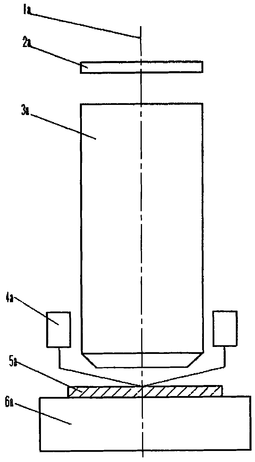
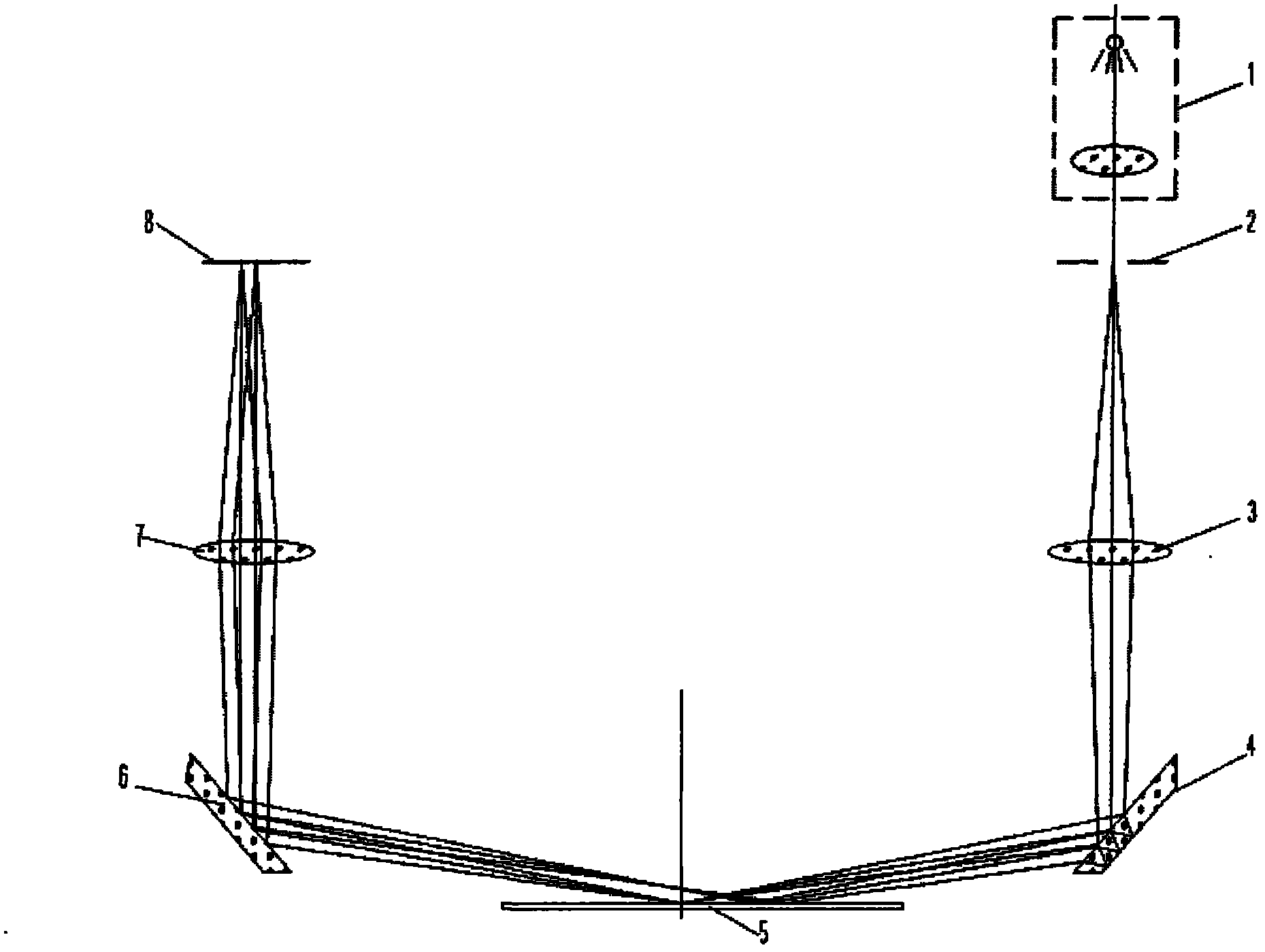
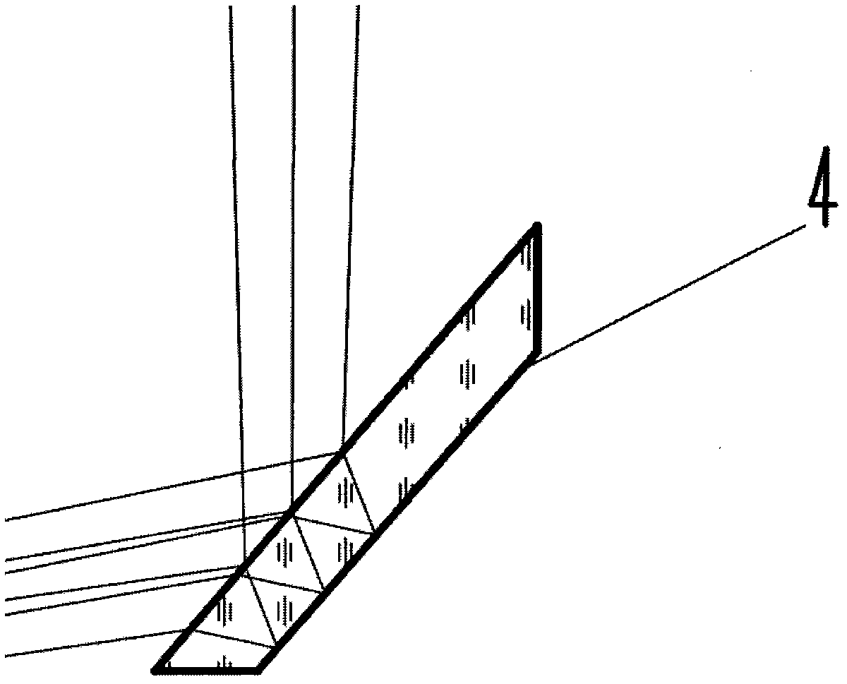
[0013] figure 1 The schematic diagram of the projection lithography machine is shown. The projection lithography machine includes an optical axis 1a, a mask plate 2a, a lithography projection objective lens 3a, a leveling and focusing detection system 4a composed of multiple focal plane detection optical systems, and a processing Object 5a and object loading platform 6a. The mask plate 2a is placed on the object plane of the lithography projection objective lens 3a, and the processing object 5a (such as silicon wafer, etc.) is placed on the object loading platform 6a. During lithography exposure, the object loading platform 6a needs to be moved so that the exposure surface of the processing object 5a is on the focal plan...


PUM


Abstract

The invention relates to an optical system for focal plane detection in projection lithography. A focus detection mark and a projection imaging system are arranged between a lighting system and a multi-reflection prism; a plane to be detected is located between the multi-reflection prism and a reflector; a focus detection mark amplification system is located between the reflector and a detector; the projection imaging system is matched with the lighting system to provide a lighting beam for lighting the focus detection mark; the multi-reflection prism is used for splitting the incident beam of the lighting system for lighting the focus detection mark into two or more detection beams with different positions; the focus detection mark can mark the position and form an image of each detection beam on the surface of the plane to be detected through the projection imaging system and multi-reflection prism; the detection beams reflected by the plane to be detected is amplified by the focus detection mark amplification system and is incident to the detector; and the detector detects the position of the reflected images amplified by the optical amplification system so as to detect the focal plane position and the focal plane inclination of a lithographic projection objective lens.

Description

technical field [0001] The invention relates to an automatic focal plane detection system, which is a technique for measuring the position movement of an imaging plane through an optical triangulation method. Background technique [0002] Photolithography device (lithography machine) is one of the important equipment for the production of large-scale integrated circuits. The projection lithography machine can image the pattern on the mask plate to the object to be processed (such as a silicon wafer, etc.) in a certain proportion through the imaging exposure device. The silicon wafer here refers to all exposed objects, including substrates, coatings and light Engraving etc. During the exposure process, it is necessary to keep the corresponding surface of the processing object (such as a silicon wafer) within the focal depth range of the exposure device. For this reason, the projection lithography machine adopts a focusing and leveling measurement system (focal plane detecti...

Claims


Application Information

Patent Timeline
Patent Type & Authority Applications(China)
IPC IPC(8): G03F9/00G03F7/20G02B27/18
Inventor 陈铭勇胡松李艳丽
Owner INST OF OPTICS & ELECTRONICS - CHINESE ACAD OF SCI
Why Eureka
Try Eureka