Supercharge Your Innovation With Domain-Expert AI Agents!

Method for oriented growth of one-dimensional inorganic nanowire array on metal substrate

A technology of metal substrates and nanowires, applied in the direction of nanotechnology, nanotechnology, nanostructure manufacturing, etc., can solve the problems of many surface defects, not very smooth, and expensive semiconductors on the surface of nanowires, and achieve simple preparation methods, The effect of cheap equipment

Inactive Publication Date: 2013-09-11
TECHNICAL INST OF PHYSICS & CHEMISTRY - CHINESE ACAD OF SCI
View PDF1 Cites 0 Cited by
  • Summary
  • Abstract
  • Description
  • Claims
  • Application Information

AI Technical Summary

Problems solved by technology

The LB self-assembly method cannot make the uneven vertical nanowires form an array; the catalyst fixed-point growth method is also prone to lodging due to the influence of the convective disturbance of the carrier gas in the growth system, and it is not easy to grow and prepare a large area, and this growth method is not easy. Realized on the metal surface; metal-catalyzed chemical etching technology is not conducive to the research and utilization of surface properties due to the high price of the original semiconductor (silicon) required, and the obtained nanowire surface has many defects and is not very smooth.

Method used


Image

  • Method for oriented growth of one-dimensional inorganic nanowire array on metal substrate
  • Method for oriented growth of one-dimensional inorganic nanowire array on metal substrate
  • Method for oriented growth of one-dimensional inorganic nanowire array on metal substrate

Examples


Embodiment 1

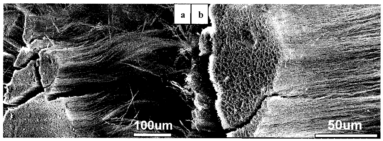
[0029] Embodiment 1, prepare SiO on Sn substrate 2 nanowire array

[0030] Take 0.2g-0.8g SiO powder, put it in a porcelain boat, put the porcelain boat in the high temperature zone of the vacuum tube furnace, take 90 grams of tin powder (the mass should be 100 times the mass of SiO, because the size of the furnace cavity is limited, so The appropriate mass of Sn that can be accommodated on both sides is about 50g) respectively placed in a porcelain boat container, placed on both sides of the high-temperature center 10-16cm, and the vacuum tube furnace is closed; the pressure in the furnace cavity is lower than 1x10 3 After Pa, argon gas is introduced until the pressure is (4-6)x10 4 Pa, and then evacuate until the pressure in the furnace chamber is lower than 1x10 3 Pa, after repeating this 3 times to ensure that the lumen is in an oxygen-free state, use argon to fill the lumen pressure to 1x10 3 Pa, sealed vacuum tube; start heating the high temperature zone of the furna...

Embodiment 2

[0032] Embodiment 2, prepare Si nanowire on Sn substrate

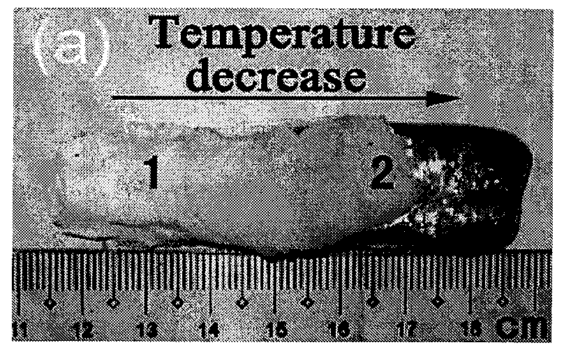
[0033] According to the method of Example 1, a hierarchical structure array of Si nanowires perpendicular to the metal tin substrate was prepared. The difference is that the amount of precursor SiO used in this example is 1.6-2g, the mass of tin powder is 80g (50 times lower than the mass of SiO), and the position is placed on both sides of the high temperature center 14-20cm area, the non-oxidizing protective gas used is argon-hydrogen mixed gas (volume ratio 95:5), and the duration of the SiO precursor in this embodiment at 1360°C is 50 minutes to 120 minutes.

[0034] The product is directly taken out from the furnace cavity, and from its optical photograph (see image 3 ) It can be seen that along the direction of temperature drop, a product with a larger area is obtained from the left side of the high temperature to the right side of the low temperature, and the obtained product area is limited by the size of the v...

Embodiment 3

[0035] Embodiment 3, prepare SiO on Sn substrate 2 Nanowire and Si nanowire composite structure array

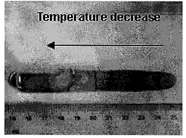
[0036] Prepare SiO perpendicular to the metal tin substrate according to the method of Example 1 2 Hierarchical composite structure arrays of nanowires and Si nanowires. The difference is: the amount of precursor SiO used in this embodiment is 0.9-1.5g, the mass of tin powder is 100g (50 times higher than SiO mass and lower than 100 times SiO mass), and it is placed at a distance In the area on both sides of the 10-20cm high temperature center, the non-oxidizing protective gas used is nitrogen, and the duration of the precursor SiO at 1360 degrees is 180 minutes to 300 minutes.

[0037] The product is directly taken out from the furnace cavity, and from its optical photos (such as Figure 5 ) It can be observed that along the direction of temperature drop, the length of the product obtained from the right side of the high temperature to the left side of the low temperatur...


PUM

PropertyMeasurementUnit
lengthaaaaaaaaaa

Abstract

The invention discloses a method for preparing a one-dimensional inorganic nanowire array in a large area on a metal substrate. The method comprises the following steps of: 1) putting a precursor into a container, putting the container into a high temperature area of a vacuum tube type stove, putting the metal substrate into the container, putting the container into a low temperature area of the vacuum tube type stove, which is 10 to 20cm away from the center of the high temperature area, making a furnace chamber of the vacuum tube type stove in an anaerobic state, filling non-oxidative protective gas into the furnace chamber until the pressure is 1*10<3>Pa, and sealing the vacuum tube type stove; and 2) raising the temperature at a rate of 10-20DEG C / minute, heating the high temperature area of the vacuum tube type stove to reach the evaporating temperature of the precursor, keeping the temperature for 30 to 300 minutes, naturally cooling to room temperature, and obtaining the vertically grown one-dimensional inorganic nanowire array on the metal substrate. By combining the chemical vaporous deposition, a Langmuir-Blodgett (LB) self-assembly technique and a catalyst fixed-point catalytic growth technique, the large-area one-dimensional inorganic nanowire array is prepared on the metal substrate by one step, and the method is suitable for growing various inorganic material arrays.

Description

technical field [0001] The invention relates to a preparation method of a one-dimensional inorganic nanometer material array, more specifically, the invention relates to a method for directional growth of a one-dimensional inorganic nanowire array on a metal substrate by a one-step method. Background technique [0002] In recent years, due to the potential important applications of semiconductor nanostructure arrays in functional nanoelectronic devices, logic gates and biosensing, the preparation research work has received extensive attention. At present, there are several important methods for the preparation of semiconductor (silicon) nanowire arrays: LB self-assembly method, catalyst fixed-point growth method and metal-catalyzed chemical etching method. Although they each have their own advantages, they also have limitations. The LB self-assembly method cannot make the uneven vertical nanowires form an array; the catalyst fixed-point growth method is also prone to lodgin...

Claims


Application Information

Patent Timeline
Patent Type & Authority Patents(China)
IPC IPC(8): B82B3/00
Inventor 张晓宏王建涛王辉欧雪梅李述汤
Owner TECHNICAL INST OF PHYSICS & CHEMISTRY - CHINESE ACAD OF SCI
Features
  • R&D
  • Intellectual Property
  • Life Sciences
  • Materials
  • Tech Scout
  • Unparalleled Data Quality
  • Higher Quality Content
  • 60% Fewer Hallucinations
Learn More