Rework method for back-side metal process

A backside metal and backside technology, applied in the direction of electrical components, semiconductor/solid-state device manufacturing, circuits, etc., can solve the problems of product scrapping, loss, abnormality, etc., and achieve the effect of ensuring yield and reliability, consistent appearance and quality

Inactive Publication Date: 2011-06-15
PEKING UNIV FOUNDER GRP CO LTD +1
View PDF0 Cites 16 Cited by
  • Summary
  • Abstract
  • Description
  • Claims
  • Application Information

AI Technical Summary

Problems solved by technology

[0004] Most of the metal on the back of the wafer is evaporated using an evaporation table. In the existing technology, the entire chip manufacturing process is basically completed after the back gold process is completed. If the metal is abnormal during the evaporation process due to various reasons, the abnormality of the process may Ultimately lead to the scrapping of the entire product, causing great losses

Method used


Image

  • Rework method for back-side metal process
  • Rework method for back-side metal process

Examples


Embodiment Construction

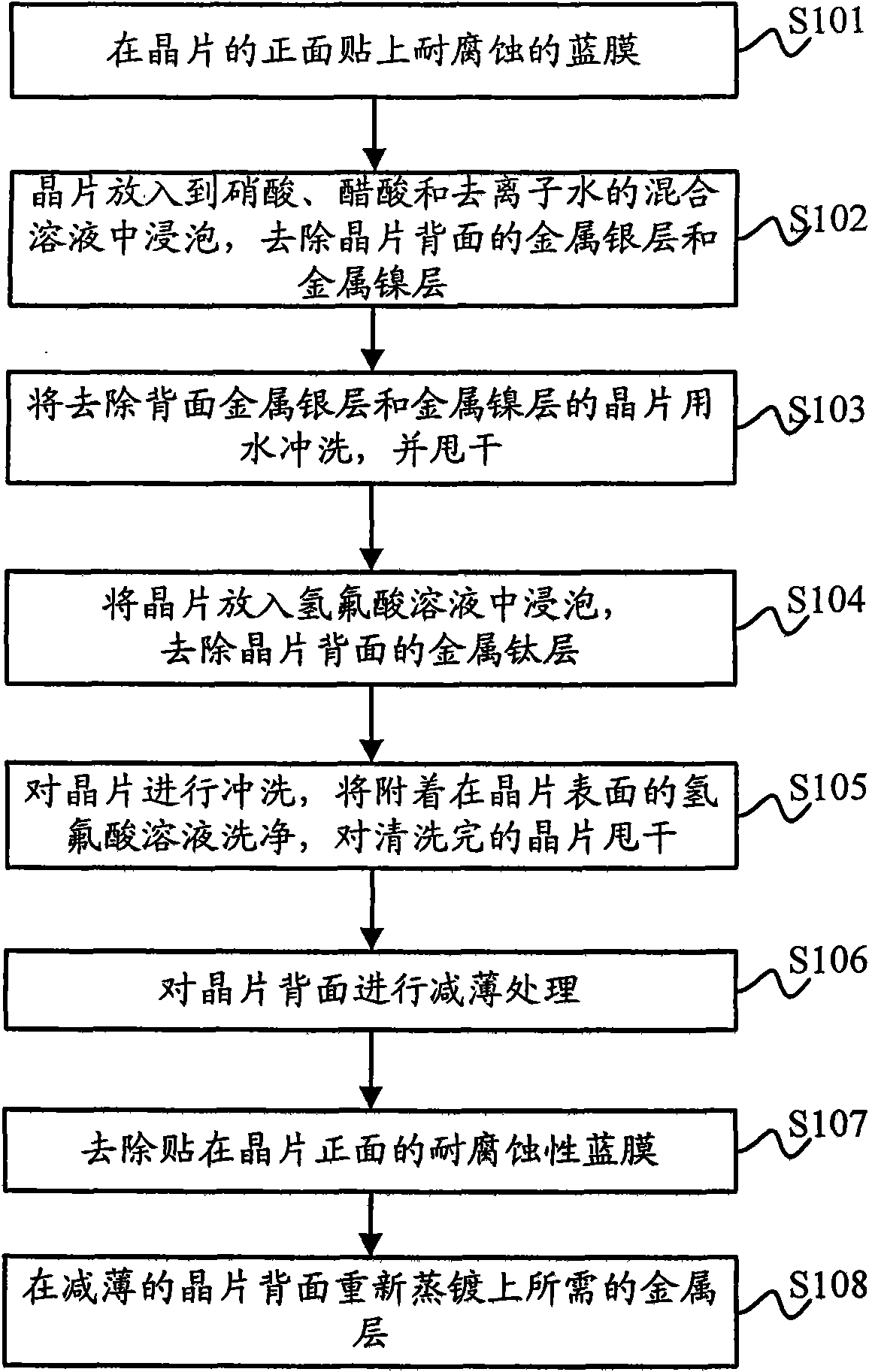
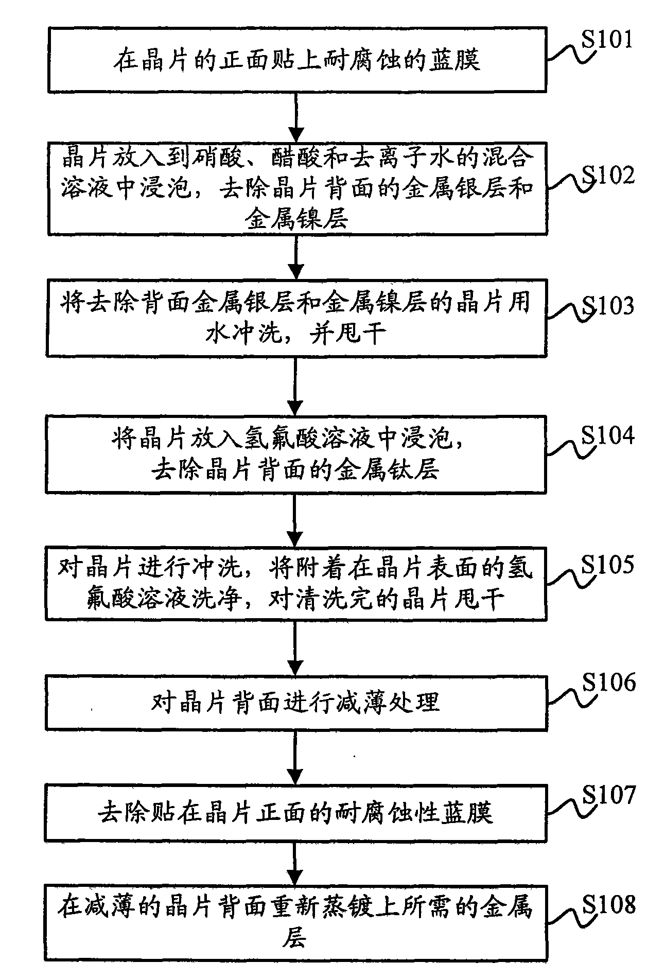
[0029] In the method for reworking the backside metal process provided by the embodiment of the present invention, the backside metal of the abnormal wafer is removed by wet etching, and the backside of the wafer from which the backside metal is removed is thinned again, and then evaporated on the backside of the wafer The required metal layer is plated. After the above process, the product that has an abnormal back metal layer can be reworked, and the requirements of normal products can be met.

[0030] A specific embodiment of the method for reworking the backside metal process provided by the present invention will be described in detail below with reference to the accompanying drawings.

[0031] In the embodiment of the present invention, in particular, a relatively common rework process of a wafer whose back metal layers are sequentially titanium (Ti), nickel (Ni) and silver (Ag) is taken as an example for illustration. However, the method for reworking the backside metal...


PUM


Abstract

The invention discloses a rework method for a back-side metal process, comprising the following steps of: removing a metal layer on the back side of a wafer to be reworked by wet etching; thinning the back side of the wafer of which the metal layer is removed; and re-evaporating the required metal layer on the back side of the thinned wafer. By adopting the embodiment, the abnormal metal layer on the back side of the wafer can be removed, the appearance and the quality of the back side of the reworked and thinned wafer can be ensured and are consistent to those of the back side of the wafer after being thinned through a normal back gold process, and the problem of metal layer stripping caused by stress on the back side of the wafer is avoided. Due to the flow, reworking on a product with the abnormal back-side metal layer already appeared is realized, and the yield and the reliability of the final product are ensured.

Description

technical field [0001] The invention relates to a semiconductor manufacturing process, in particular to a rework method for a back metal process. Background technique [0002] At present, metal-oxide-semiconductor (Metal Oxide Semiconductor, MOS) field-effect transistors, referred to as MOS transistors, and other devices using ultra-thin chips have been widely used in the semiconductor field, especially in smart cards, radio frequency identification (Radio Frequency Identification (RFID) devices, new mobile phones, personal digital assistants (Personal Digital Assistant, PDA) and other small, light and powerful electronic devices are more widely used. [0003] In the manufacturing process of power MOS tubes and other devices, it is usually necessary to thin the wafer and then carry out back metallization, the main purpose of which is to reduce the contact resistance. However, metal peeling will occur due to stress between the metal layer and the silicon substrate. Therefor...

Claims


Application Information

Patent Timeline
Patent Type & Authority Applications(China)
IPC IPC(8): H01L21/00
Inventor 李熙胡德明
Owner PEKING UNIV FOUNDER GRP CO LTD
Why Eureka
Try Eureka