Bipolar transistor

A technology of bipolar transistors and transistors, which is applied in the manufacture of transistors, semiconductor devices, semiconductor/solid-state devices, etc., can solve the problems of large device area, high cost, and complex deep trench isolation process, etc., to reduce the device area and reduce parasitic effects , the effect of reducing the number of photolithography layers

Active Publication Date: 2011-06-22
SHANGHAI HUAHONG GRACE SEMICON MFG CORP
View PDF0 Cites 32 Cited by
  • Summary
  • Abstract
  • Description
  • Claims
  • Application Information

AI Technical Summary

Problems solved by technology

[0004] The existing bipolar transistor technology is mature and reliable, but the main disadvantages are: 1. The epitaxy cost of the collector area is high; 2. The formation of collector pick-up depends on high-dose and high-energy ion implantation to lead out the buried layer of the collector area. , so it occupies a large device area; 3. The deep trench isolation process is complex and costly; 4. The number of photolithography layers in the transistor process is large

Method used


Image

  • Bipolar transistor
  • Bipolar transistor
  • Bipolar transistor

Examples


Embodiment Construction

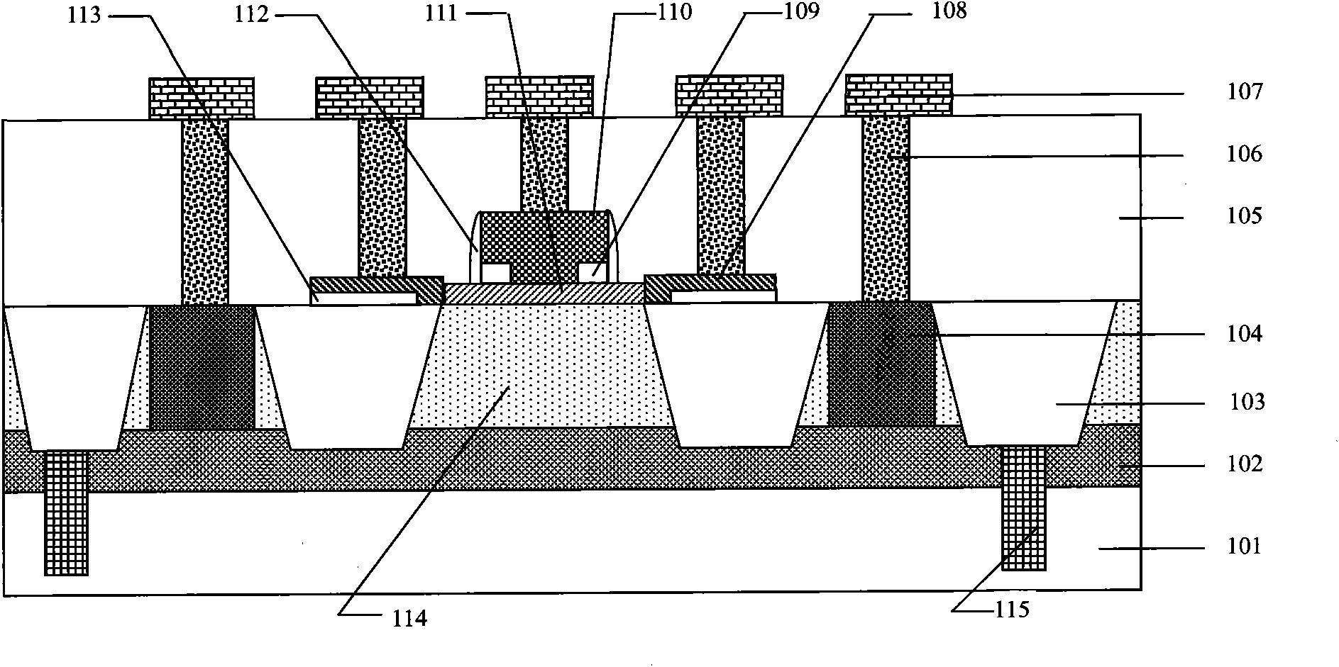
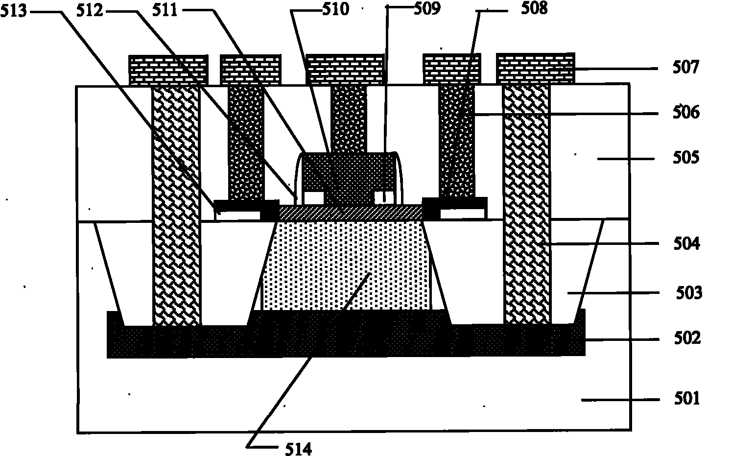
[0017] Such as figure 2 As shown, it is a schematic diagram of the device structure of the bipolar transistor of the present invention. An active region isolated by a shallow trench field oxygen 503 is formed on a silicon substrate 501. The bipolar transistor includes: a collector region 514, a base region 511, A launch area 510 .

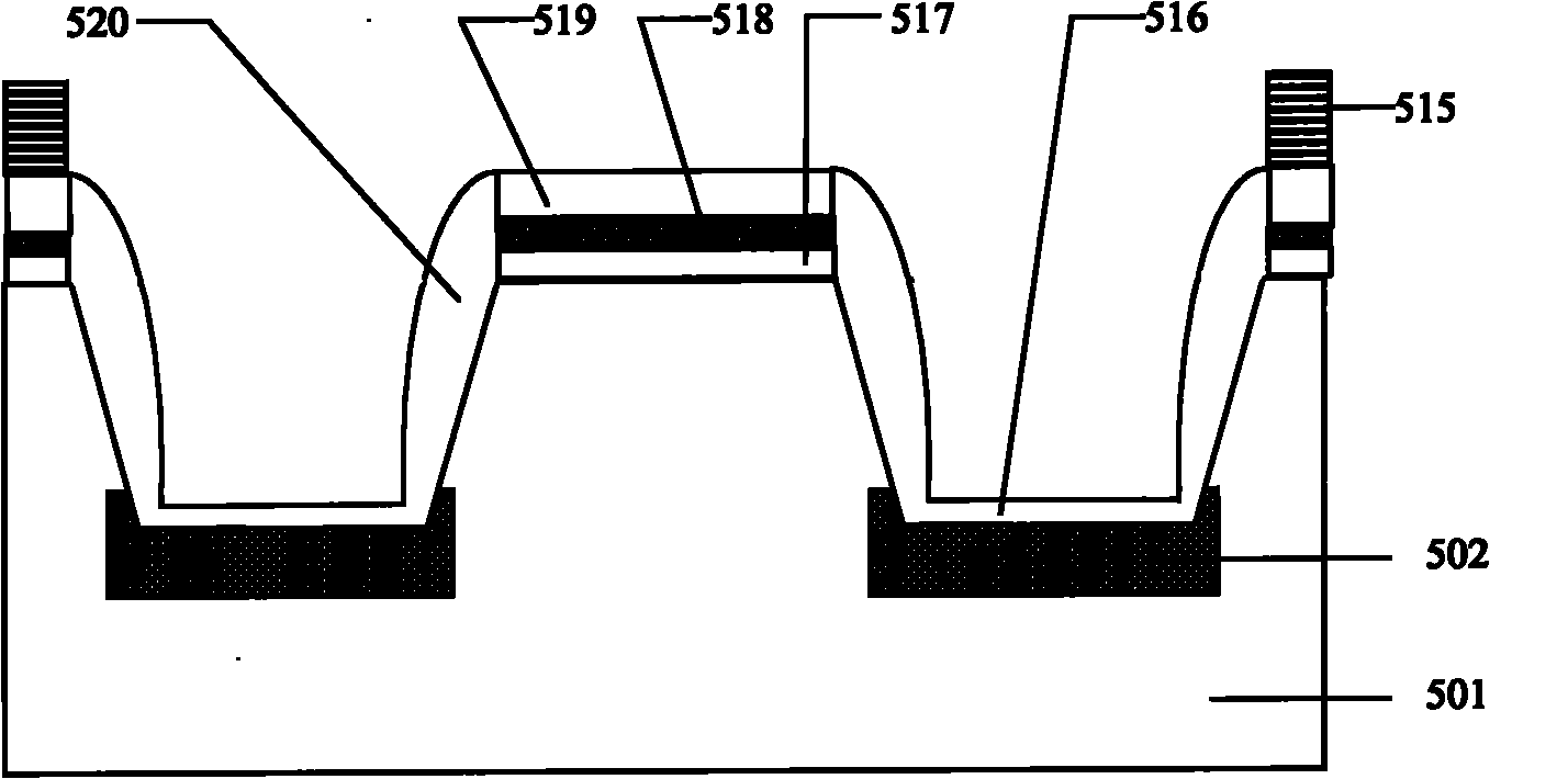
[0018] The collector region 514 is formed by performing single-step or multi-step implantation of impurity ions of the first conductivity type in the active region. The bottom of the collector region 514 is connected to a buried layer formed by connecting two pseudo-buried layers 502 at the bottom of shallow grooves on both sides of the active region; when the active region is smaller than 0.5 microns, the two pseudo-buried layers 502 Intersect in the active region by lateral diffusion to form the buried layer of the collector region 514; when the active region is greater than 0.5 microns, implant at the same depth as the two pseudo-buried layers...


PUM


Abstract

The invention discloses a bipolar transistor. An active area is isolated by shallow-trench field oxide. The bipolar transistor comprises a collector region, a base region and a transmission region, wherein the collector region is formed by a first conductive type foreign ion injection layer which are formed in the active area, and a buried layer formed by connection of two first conductive type pseudo-buried layers is connected to the bottom of the collector region, and the pseudo-buried layer is formed by injecting first conductive type foreign ions which are injected from the bottom of trenches at two sides of the active area; deep groove contact is manufactured in field oxide on the pseudo-buried layer to lead out a collector; the base region is formed by a second conductive type film which is formed on the collector region; and the transmission region is formed by first conductive type polycrystalline silicon which is formed on the base region. The bipolar transistor can reduce the device area, the parasitic effect, the number of photoetching layers and the process cost.

Description

technical field [0001] The invention relates to a semiconductor integrated circuit device, in particular to a bipolar transistor. Background technique [0002] In radio frequency applications, higher and higher device characteristic frequencies are required. Although RFCMOS can achieve higher frequencies in advanced process technologies, it is still difficult to fully meet radio frequency requirements. For example, it is difficult to achieve characteristic frequencies above 40GHz, and advanced technology The research and development cost of compound semiconductors is also very high; compound semiconductors can realize very high characteristic frequency devices, but due to the disadvantages of high material cost and small size, and the toxicity of most compound semiconductors, its application is limited. Si bipolar junction transistors (BJT) or SiGe heterojunction bipolar transistors (HBT) are good choices for UHF devices. [0003] Taking the NPN transistor as an example, th...

Claims


Application Information

Patent Timeline
Patent Type & Authority Applications(China)
IPC IPC(8): H01L29/73H01L29/06H01L21/331
CPCH01L29/41708H01L29/732H01L29/66287H01L29/0821H01L21/76232
Inventor 邱慈云朱东园钱文生范永洁
Owner SHANGHAI HUAHONG GRACE SEMICON MFG CORP
Why Eureka
Try Eureka