TFT-LCD array substrate, and method and equipment for detecting size of multi-layer pattern
An array substrate and graphics technology, applied in optics, instruments, electrical components, etc., can solve problems affecting production efficiency, production time delay, cumbersome detection process, etc., and achieve the effects of improving efficiency and accuracy, simple preparation, and easy implementation
- Summary
- Abstract
- Description
- Claims
- Application Information
AI Technical Summary
Problems solved by technology
Method used
Image
Examples
Embodiment 1
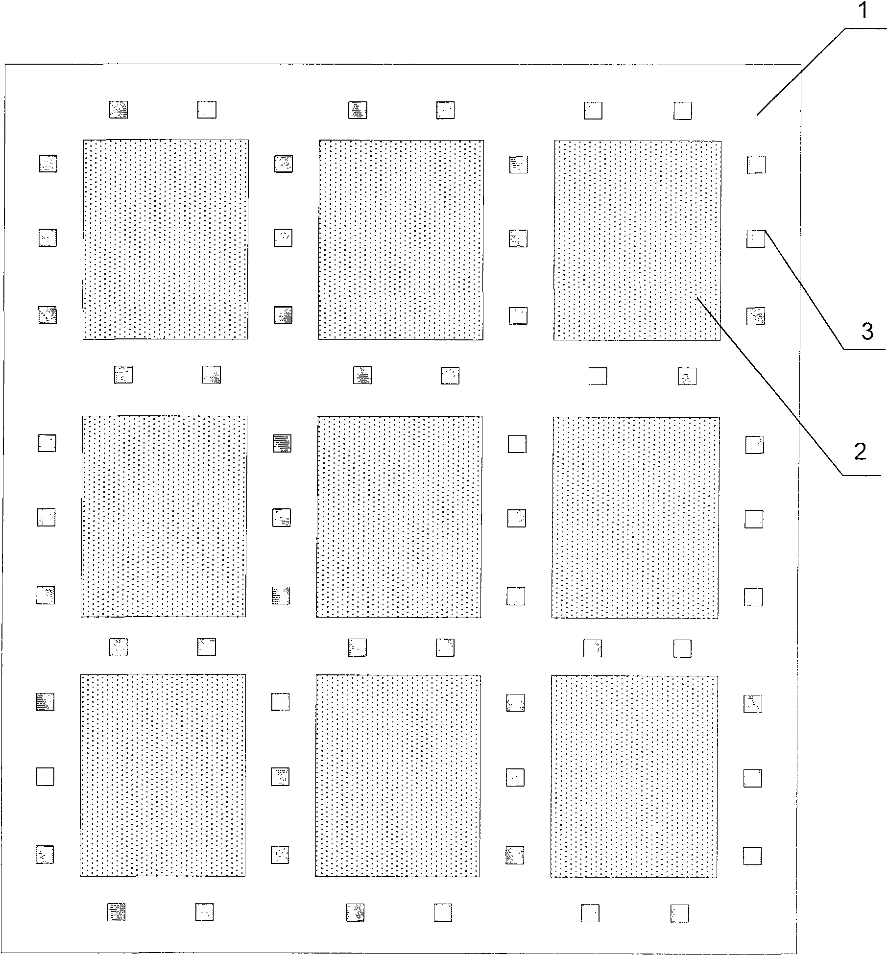
[0049] An embodiment of the present invention provides a TFT-LCD array substrate, such as figure 1 As shown, the array substrate includes: a substrate 1 and a multilayer array pattern 2 formed on the substrate 1, and the area on the substrate 1 where the multilayer array pattern 2 is not provided is provided with The detection mark 3 of the size of each array pattern in the layer array pattern 2, the detection mark 3 includes: a detection pattern set on the same layer as the pattern to be detected and having the same size, and a detection liner set on a different layer from the detection pattern end.
[0050] In order to facilitate the detection and alignment detection of the array pattern of each layer of the TFT-LCD array substrate, the embodiment of the present invention provides the array substrate with the above structure. Specifically, the array substrate with the above-mentioned structure is irradiated with direct light, and the line width of each layer of graphics can...
Embodiment 2
[0055] In the production process of the array substrate, for the structures of the array patterns of different layers, a plurality of different detection marks for detecting the array patterns of different layers can be formed.
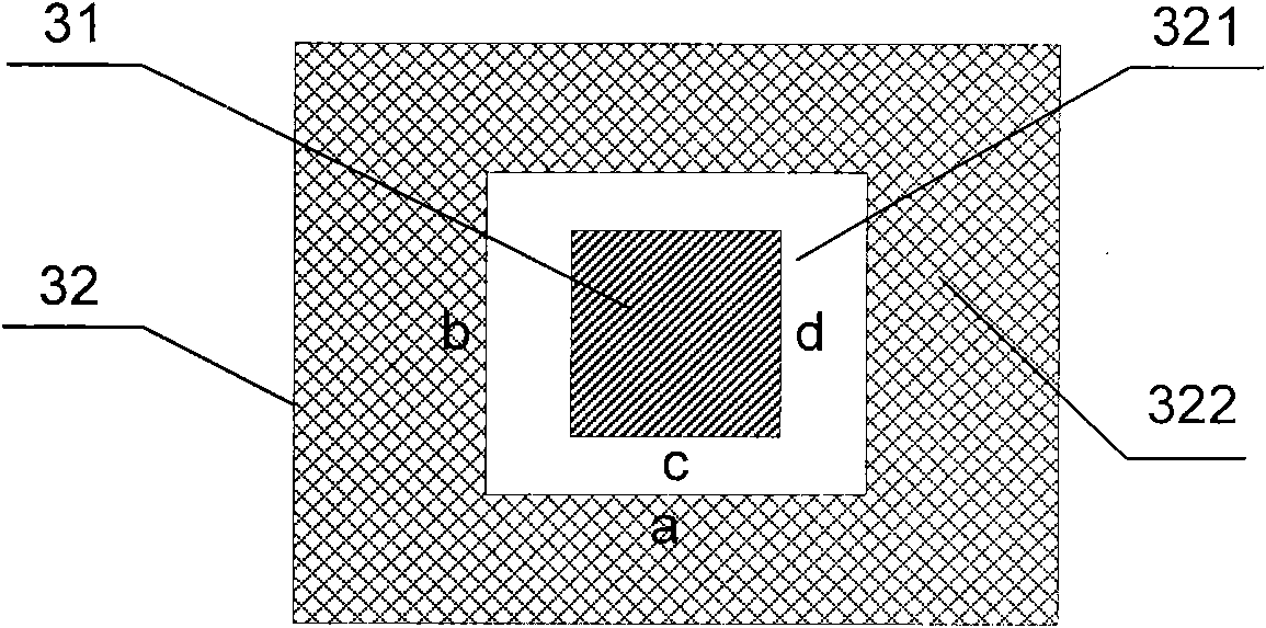
[0056] On the basis of Embodiment 1, further, the detection mark can be a transmission detection mark, such as figure 2 As shown, the detection substrate 32 includes: a light-transmitting detection window 321 located in the central area of the detection substrate 32 , and a light-shielding window frame 322 .
[0057] The technical solution of the embodiment of the present invention will be described below by taking the detection of the line width of the data line in the traditional TFT-LCD array structure as an example. Such as figure 2 As shown, the detection mark includes: a detection pattern 31 disposed on the same layer as the data line and having the same size, and a detection substrate 32 disposed on a different layer from the detection pat...
Embodiment 3
[0063] On the basis of Embodiment 1, further, the detection mark can be a reflective detection mark, such as Figure 4 As shown, that is, the detection pattern 31 shields light, and the detection substrate 32 reflects light.
[0064] Wherein, the detection substrate 32 can be arranged on the same layer as the array pattern other than the array pattern to be detected, or it can be arranged on the same layer as the array pattern by using a separate preparation process. In this embodiment, the detection substrate 32 and the grid Take the line same layer setting as an example to illustrate. Form a light-shielding detection pattern 31 that is arranged on the same layer as the detected array pattern and has the same size. A detection substrate 32 lining the position below the detection pattern 31 is formed, that is, the detection substrate 32 is arranged on the same layer as the gate lines.
[0065] During detection, direct light is used to irradiate the detection mark vertically ...
PUM
 Abstract
Description
Claims
Application Information


