Microprobe structure and manufacturing method thereof

A manufacturing method and micro-probe technology, which are applied in the directions of measuring devices, instruments, measuring electricity, etc., can solve the problems of lowering the strength of the probe card, increasing the impedance, and being unsuitable for high-frequency testing.

Inactive Publication Date: 2011-07-13
PREMTEK INT
View PDF14 Cites 32 Cited by
  • Summary
  • Abstract
  • Description
  • Claims
  • Application Information

AI Technical Summary

Problems solved by technology

However, as we all know, silicon is a brittle material, and its material strength on a specific crystal plane is weak, and the number of contacts (touch-down number) will be low; and its electrical signal is only transmitted by a thin film, which will lead to increased impedance and a very high load. easy to overshoot and short circuit
In short, the reliability of this type of probe card will not meet the needs of the industry
[0005] In U.S. Patent No. 5,476,211 and U.S. Patent No. 5,926,951, a method for manufacturing a microelectronic component spring interconnection assembly is disclosed. However, this type of probe card is difficult to withstand lateral stress, and the microsprings are interconnected. Even the components are long, therefore, not suitable for high-frequency testing
[0006] Also, in U.S. Patent No. 2007 / 0024298A1, a torsion spring probe (torsion spring probe) is proposed, and each probe is designed with a micro torsion bar (torsion bar) to overcome the lateral stress, and then This will limit the fine pitch development capability of this type of probe card
[0007] In addition, in the Invention Announcement / Publication No. I279556 of the Taiwan Patent Gazette of China, a micro-elastic contactor whose micro-stepped cantilever beam design can strengthen the force of the micro-probe, but the area occupied by the second sacrificial layer metal is quite large , it is necessary to reduce the residual stress caused by electroplating as much as possible, otherwise it is easy to reduce the strength of this type of probe card

Method used


Image

  • Microprobe structure and manufacturing method thereof
  • Microprobe structure and manufacturing method thereof
  • Microprobe structure and manufacturing method thereof

Examples


Embodiment Construction

[0052] The implementation of the present invention will be described in more detail below in conjunction with the accompanying drawings, so that those skilled in the art can implement it after studying this specification.

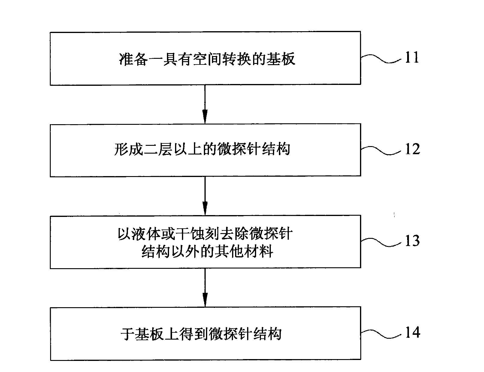
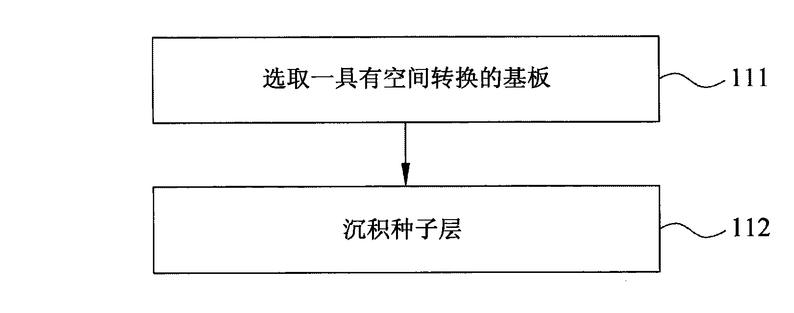
[0053] figure 1 It is a flowchart for illustrating the process steps of the manufacturing method of the microprobe structure of the present invention. Such as figure 1 Shown in is the manufacturing method of the micro-probe structure of the present invention. Firstly, in step 11, a substrate with space conversion is prepared to facilitate subsequent formation of the micro-probe structure on the substrate, and then proceed to step 12.

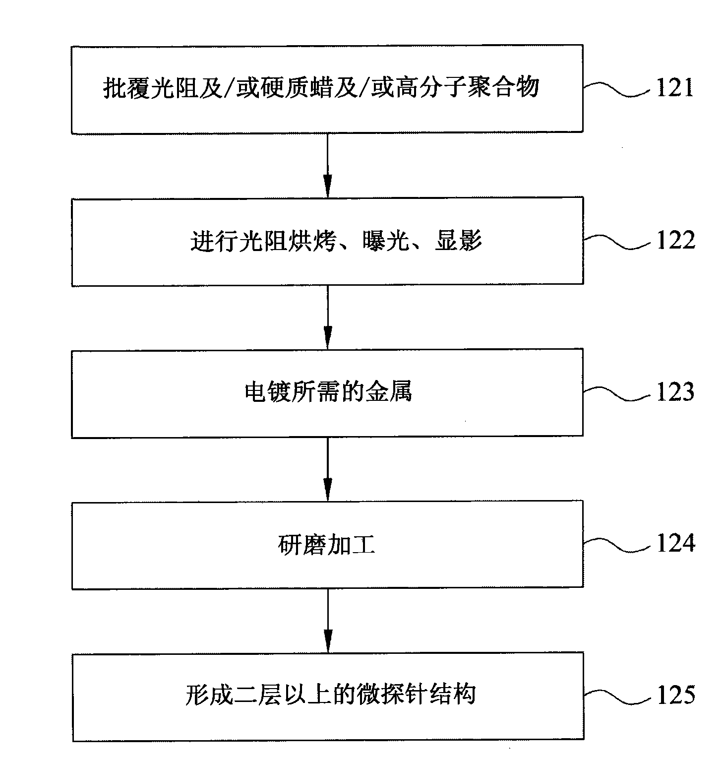
[0054] In step 12, using the lithography, electroplating, planarization, and etching technologies of the semiconductor manufacturing process, and replacing the metal plating of the second sacrificial layer with polymers, a micro-metal structure of more than two layers is successively formed on the surface of the substrate, h...


PUM


Abstract

The invention discloses a microprobe structure and a manufacturing method thereof. The microprobe structure is suitable for a probe card component used for test of an electronic component. The manufacturing method for the microprobe comprises that: a micro metal structure with over two layers is sequentially formed on the surface of a substrate with space conversion by lithography, electroplating, planarization and etching technologies of a semiconductor manufacture procedure and in a way that a macromolecule substitutes and electroplates a second sacrificial layer metal and then the microprobe structure of the micro metal structure with over two layers is obtained, wherein each layer of micro metal structure is made of one material and the micro metal structure with over two layers can be made of the same material and / or different materials. The microprobe structure manufactured by the manufacturing method has a structural design of a reinforced cantilever, is suitable for a component used for test of various electronic components, and can serve as a test head of a probe card to effectively increase test bandwidth, reduce space and improve parallel test capability.

Description

technical field [0001] The invention relates to a probe structure and a manufacturing method thereof, in particular to a microprobe structure suitable for a probe card assembly used for testing electronic components and a manufacturing method thereof. Background technique [0002] The probe card is used in integrated circuit IC before packaging, to do functional test on the bare chip with probes, so as to screen out defective products, and then carry out the subsequent packaging project. Therefore, it is an important process in the manufacture of integrated circuits that has a considerable impact on the manufacturing cost. In short, the probe card is the interface between a test machine and the wafer. Each integrated circuit IC needs at least one corresponding probe card. The purpose of the test is to make the good products enter the The next packaging process and avoid waste caused by continued processing of defective products. Therefore, high reliability is a very import...

Claims


Application Information

Patent Timeline
IPC IPC(8): G01R1/073
Inventor 王宏杰黄雅如
Owner PREMTEK INT
Why Eureka
Try Eureka