Laser direct-writing device

A technology of laser direct writing and laser interferometer, which is used in photoplate-making process exposure devices, laser welding equipment, microlithography exposure equipment, etc. Micro-nano graphics and other problems, to achieve the effect of high-precision and rapid writing

Inactive Publication Date: 2011-07-13
SHANGHAI INST OF OPTICS & FINE MECHANICS CHINESE ACAD OF SCI
View PDF7 Cites 29 Cited by
  • Summary
  • Abstract
  • Description
  • Claims
  • Application Information

AI Technical Summary

Problems solved by technology

[0004] (1) Modular laser direct engraving device (see the invention patent "Modular laser direct engraving device", patent number CN200720072320), in which the piezoelectric ceramic (hereinafter referred to as PZT) displacement stage is used as the sample stage, which has a high Position accuracy, but due to the limitation of the displacement principle of PZT, its motion range is only in the micron level, and it is difficult to reach the millimeter level. It can only be used as a laboratory research platform, and it cannot be used to process and produce micro-nano devices with practical applications;
[0005] (2) Laser direct writing equipment integrating rectangular coordinates and polar coordinates (see "Acta Photonica Sinica", Volume 31, Issue 5, 2002). This device has the ability to write binary optical elements in a large range, but it can only describe relatively simple The lines do not have the ability to process complex micro-nano graphics, so its application range is also very limited

Method used


Image

  • Laser direct-writing device
  • Laser direct-writing device
  • Laser direct-writing device

Examples


Embodiment Construction

[0020] The present invention will be further described in detail below in conjunction with the examples.

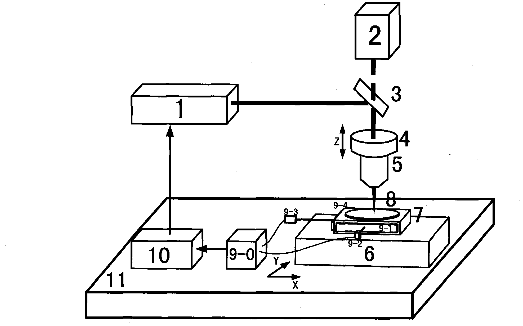
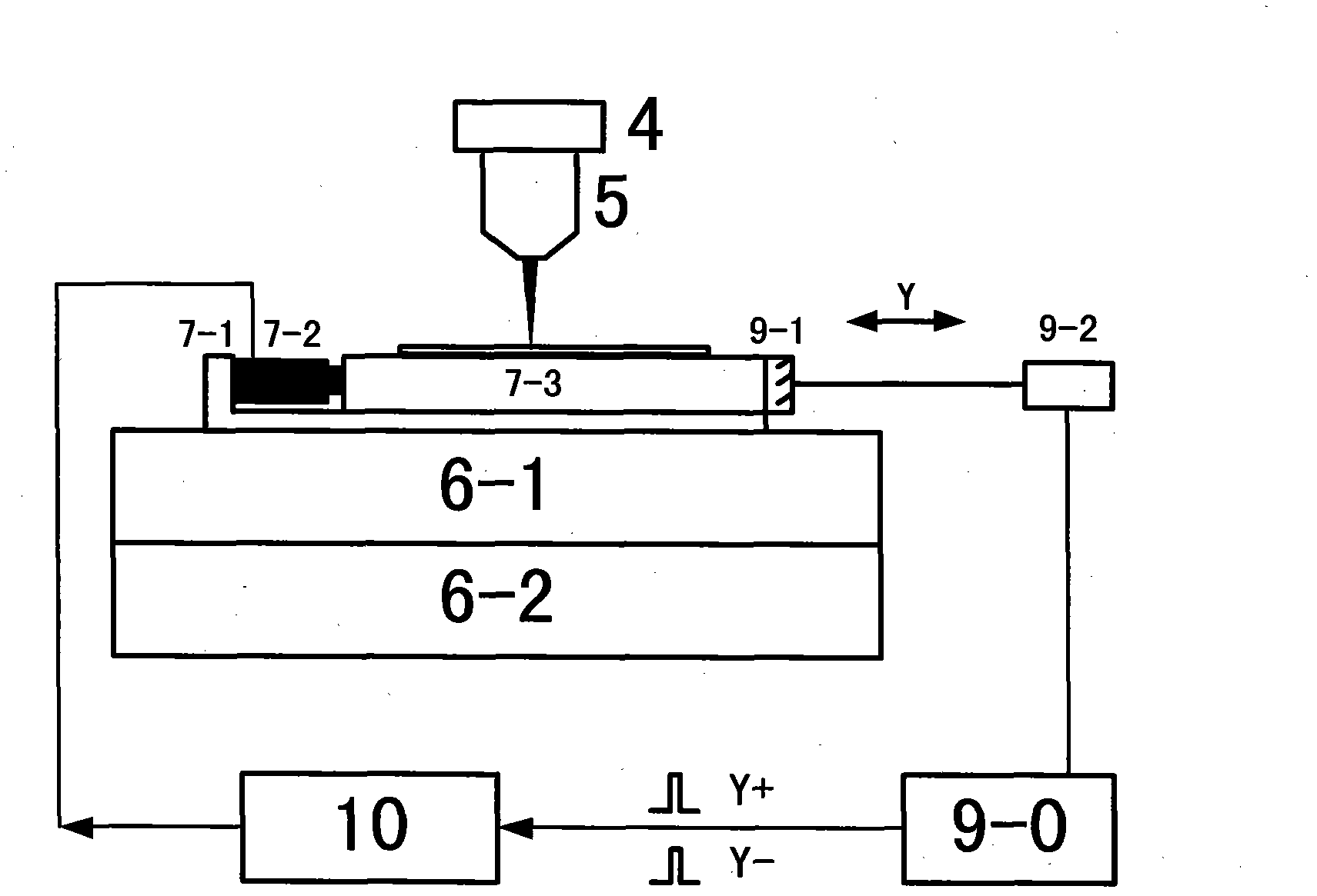
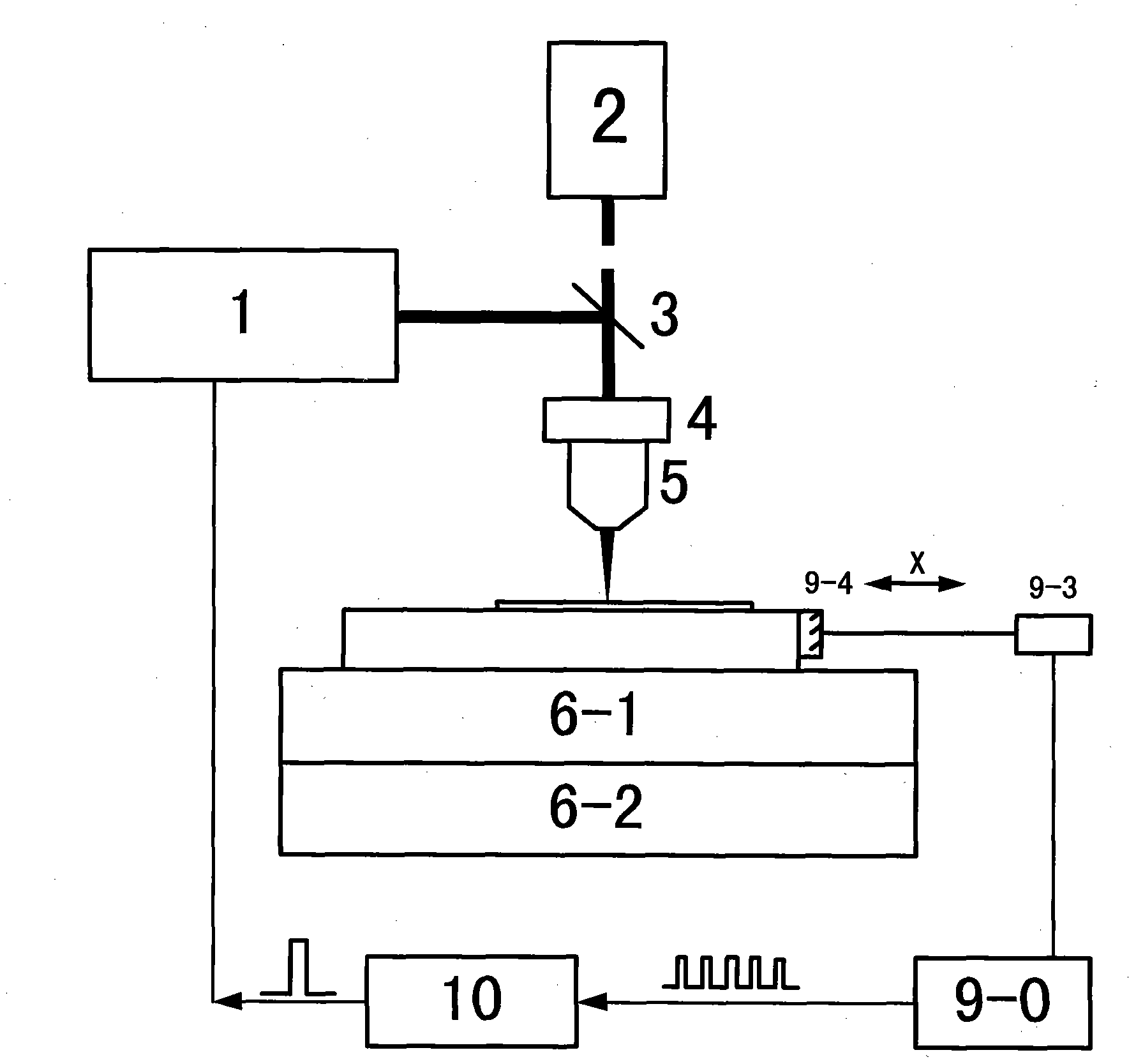
[0021] Such as figure 1 , The laser direct writing device of the present invention includes a writing light source 1, a defocus detection module 2, a spectral beam splitter 3, a focusing PZT4, an objective lens 5, a two-dimensional XY motor platform 6, a Y-axis correction platform 7, a sample to be engraved 8, a laser Interferometer 9, master controller 10 and anti-vibration table 11, the positional relationship of above-mentioned parts is as follows:

[0022] The two-dimensional XY motor platform 6 and the general controller 10 are set on the anti-vibration table 11, the Y-axis correction platform 7 is fixed on the two-dimensional XY motor platform 6, and the samples to be engraved 8 are placed On the Y-axis correction platform 7, the writing light source 1 and the defocus detection module 2 are respectively located on both sides of the spectral beam splitter 3, and the...


PUM


Abstract

The invention relates to a laser direct-writing device; the laser direct-writing device is firstly characterized by comprising an inscribing light source, a out-of-focus detection module, a spectrum spectroscope, a focusing PZT (Piezoelectric Transducer), an object lens, a two-dimensional XY motor platform, a Y-axis correcting platform, a sample to be inscribed, a laser interferometer, a master controller and a shockproof platform, wherein a combined structure of the large-stroke two-dimensional XY motor platform and the small-stroke Y-axis correcting platform is adopted as a sample displacement platform; laser direct-writing device is secondly characterized in that the laser interferometer is used for measuring the change of the distance between the X-axis and the Y-axis, and the synchronization of the movement of the X-axis and the laser pulse as well as the accurate correction of the Y-axis during the moving process of the X-axis can be simultaneously realized by using the position pulse signal emitted from the laser interferometer. The laser direct-writing device can realize quick high-precision inscribing within a large range, thereby being capable of inscribing micro-nano graphs and structures in any shape within a large range and having relatively higher practical value.

Description

technical field [0001] The invention is a large-scale laser direct writing device, which is mainly applicable to the field of micro-nano processing. Background technique [0002] Laser direct writing technology is a technology that condenses laser beams into extremely small light spots to act on photosensitive or heat-sensitive thin film materials to directly generate micro-nano patterns. Compared with other micro-nano processing methods, it has many advantages such as low cost, short processing cycle, flexible use, and low environmental requirements. Laser direct writing technology has been widely used in the production of microelectronics, integrated optics (DOEs), microelectromechanical systems (MEMs), hybrid integrated circuits, and microwave integrated circuits. It is a practical technology with broad development prospects. [0003] In the prior art, there are the following laser direct writing devices: [0004] (1) Modular laser direct engraving device (see the inven...

Claims


Application Information

Patent Timeline
IPC IPC(8): G03F7/20B23K26/00B23K26/02B23K26/08B23K26/046B23K26/36
Inventor 范永涛徐文东郝春宁刘前
Owner SHANGHAI INST OF OPTICS & FINE MECHANICS CHINESE ACAD OF SCI
Why Eureka
Try Eureka