Solid-state memory device and method for arrangement of solid-state memory cells

a solid-state memory and memory cell technology, applied in semiconductor devices, digital storage, instruments, etc., can solve problems such as preventing high-capacity memory devices, and achieve the effect of simple structure and rapid writing

Active Publication Date: 2005-10-27
SONY CORP
View PDF9 Cites 15 Cited by
  • Summary
  • Abstract
  • Description
  • Claims
  • Application Information

AI Technical Summary

Benefits of technology

[0056] As mentioned above, the MRAM composed of TMR elements is a non-volatile RAM which is simple in structure and is capable of rapid writing through reversal of magnetic moment. For the high-capacity (high-integrated) memory to be produced in high yields for practical use, it is necessary that the TMR elements should be uniform in writing and reading characteristics so that the writing and reading operations can be performed with a broad margin.

Problems solved by technology

This is a hindrance to a high-capacity memory device.

Method used


Image

  • Solid-state memory device and method for arrangement of solid-state memory cells
  • Solid-state memory device and method for arrangement of solid-state memory cells
  • Solid-state memory device and method for arrangement of solid-state memory cells

Examples


embodiment 1

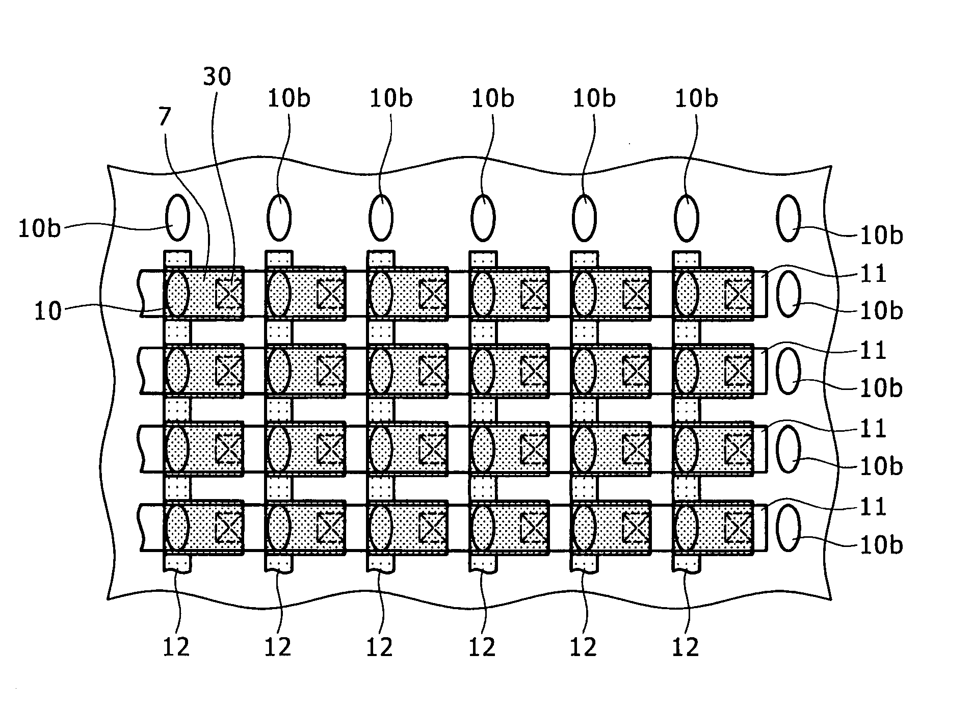
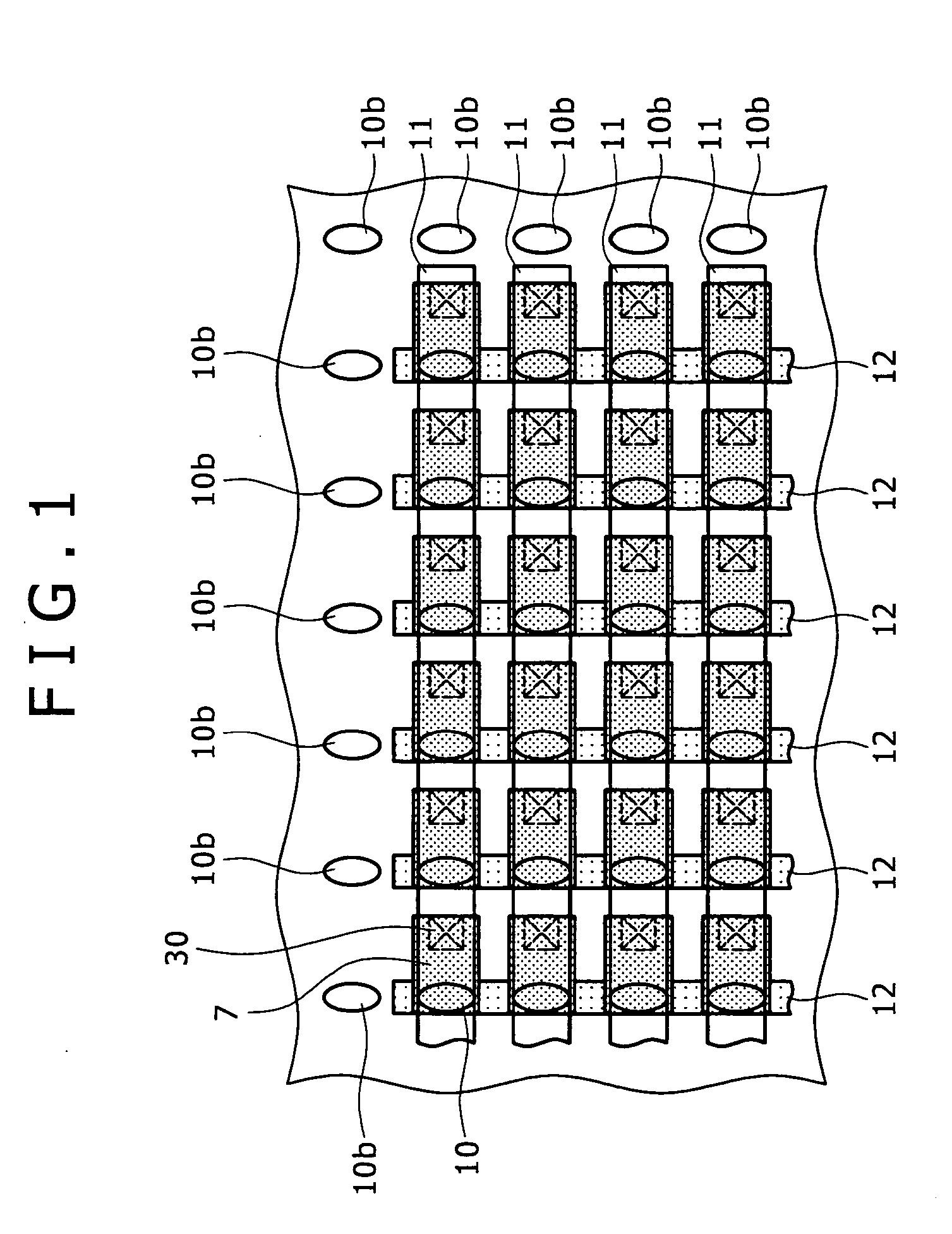
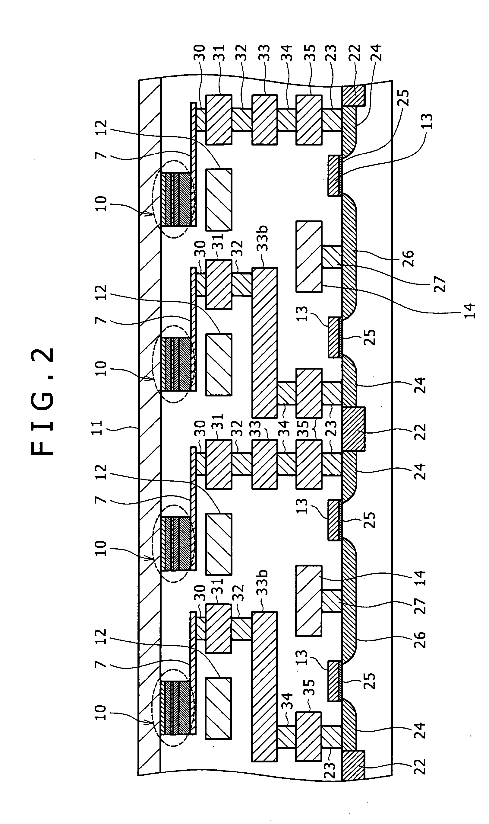
[0104]FIG. 1 is a plan view showing the arrangement of memory cells in the magnetic memory device (MRAM) according to the first embodiment. This magnetic memory device is comparable to MRAM of related art. As in FIG. 15, FIG. 1 does not show, for brevity, the wirings and the transistors for reading (selection) which are formed in the lower layer.

[0105] The MRAM shown in FIG. 1 is identical with the related-art MRAM shown in FIG. 15 in that each memory cell is that of 1T1J type which has one TMR element 10 and one transistor for reading (selection). Each memory cell also includes the lead wiring 7 which extends from the leading electrode 6 of the TMR element 10 and the reading connecting plug 30 which connects the lead wiring 7 to the drain electrode of the transistor for reading (selection). It further includes the bit lines 11 and the writing word lines 12 which are connected to individual memory cells.

[0106] The difference between the two resides in the arrangement of memory cel...

embodiment 2

[0119]FIG. 3 is a plan view showing the arrangement of memory cells in the magnetic memory device (MRAM) according to the second embodiment.

[0120] The MRAM shown in FIG. 3 is identical with the MRAM shown in FIG. 1 according to Embodiment 1 in that each memory cell is that of 1T1J type which has one TMR element 10 and one transistor for reading (selection). Each memory cell also includes the lead wiring 7 which extends from the leading electrode 6 of the TMR element 10 and the reading connecting plug 30 which connects the lead wiring 7 to the drain electrode of the transistor for reading (selection). It further includes the bit lines 11 and the writing word lines 12 which are connected to individual memory cells. As in FIG. 1, FIG. 3 does not show, for brevity, the wirings and the transistors for reading (selection) which are formed in the lower layer.

[0121] This embodiment differs from Embodiment 1 in the way of arrangement. In Embodiment 1, the TMR elements 10 in all the columns...

embodiment 3

[0126]FIG. 4 is a plan view showing the arrangement of memory cells in the magnetic memory device (MRAM) according to this embodiment. The MRAM shown in FIG. 4 is identical with the MRAM shown in FIG. 1 according to Embodiment 1 in that each memory cell is that of 1T1J type which has one TMR element 10 and one transistor for reading (selection). Each memory cell also includes the lead wiring 7 which extends from the leading electrode 6 of the TMR element 10 and the reading connecting plug 30 which connects the lead wiring 7 to the drain electrode of the transistor for reading (selection). It further includes the bit lines 11 and the writing word lines 12 which are connected to individual memory cells. As in FIG. 1, FIG. 4 does not show, for brevity, the wirings and the transistors for reading (selection) which are formed in the lower layer.

[0127] The difference between Embodiment 3 and Embodiment 1 resides in the way of arrangement. The arrangement in Embodiment 1 is such that the ...


PUM


Abstract

A high-capacity magnetic memory device in which the magnetic field for writing is nearly uniform for all memory elements. It is realized by reducing the deformation of resist pattern which occurs in photolithography when mask patterns are close to each other. The magnetic memory device is an MRAM composed of a large number of memory cells, each including one TMR element, one transistor for reading (selection), and reading plugs that connect the TMR element to the transistor for reading (selection). These memory cells are arranged such that the TMR elements are in a pattern of translational symmetry. For writing, memory cells are connected by the bit lines and the writing word lines which intersect orthogonally. The long axis of the TMR element is oriented aslant 45° with respect to these lines, so that the TMR elements are capable of toggle-mode writing.

Description

BACKGROUND OF THE INVENTION [0001] The present invention relates to a solid-state memory device to be produced by lithography and a method for arrangements of solid-state memory cells. The solid-state memory device includes MRAM (Magnetic Random Access Memory), DRAM (Dynamic Random Access Memory), SRAM (Static Random Access Memory), FRAM (Ferroelectric Random Access Memory), ROM (Read Only Memory), PROM (Programmable ROM), and EPROM (Erasable and Programmable ROM). More particularly, the present invention relates to the array pattern of the information storing parts of memory elements. [0002] The recent wide spread of information and communications equipment, particularly personal small ones such as portable terminals, requires their constituents such as memory and logic elements to have improved performance, including high integration, high speed, and low power consumption. [0003] Especially, non-volatile memory is regarded as indispensable in the age of ubiquitous computing becaus...

Claims


Application Information

Patent Timeline
Patent Type & Authority Applications(United States)
IPC IPC(8): G11C11/15G11C5/02G11C11/00G11C11/16H01L21/8239H01L21/8246H01L27/105H01L27/22H01L43/08
CPCB82Y10/00G11C5/025H01L27/228G11C11/16G11C11/15H10B61/22
Inventor MOTOYOSHI, MAKOTO
Owner SONY CORP
Why Eureka
Try Eureka