Method and system for manufacturing component by using shadow mask technological line

A production line and technical technology, applied in semiconductor/solid-state device manufacturing, electrical components, ion implantation plating, etc., can solve problems such as inability to manufacture microelectronic components

Inactive Publication Date: 2011-07-13
潘重光
3 Cites 2 Cited by

AI-Extracted Technical Summary

Problems solved by technology

[0006] The first purpose of the present invention is to provide a method for manufacturing devices using a shadow mask technology production line ...

Method used

F, the substrate is pushed into the annealing vacuum box, and annealing is carried out; specifically, it eliminates the stress generated in the deposition event, stabilizes the size, r...

Abstract

The invention discloses a method and a system for manufacturing a component by using a shadow mask technological line. The method comprises the following steps: A. firstly depositing materials in a vacuum deposition box, and then accurately locating shadow mask plates in a first area of a substrate according to the operable relationship between the shadow mask plates and deposited material sources which are fully positioned in the vacuum deposition box; B. depositing the materials on the first area of the substrate through vacuum evaporation to form a graph; C. accurately locating the shadow mask plates and the deposited material sources in a second area of the substrate by a transmission device; and D. depositing the materials on the second area of the substrate through vacuum evaporation to form a graph and stereoscopic overlap of the materials; repeating step C and D according to design so as to complete composition and connection of the component; and sequentially annealing, testing, cutting and assembling respectively by a vacuum annealing box, a vacuum test box, a vacuum cutting box and a vacuum assembling box, and finally forming the complete component.

Application Domain

Vacuum evaporation coatingSputtering coating +2

Technology Topic

EngineeringVacuum deposition +4

Image

  • Method and system for manufacturing component by using shadow mask technological line
  • Method and system for manufacturing component by using shadow mask technological line
  • Method and system for manufacturing component by using shadow mask technological line

Examples

  • Experimental program(1)
  • Effect test(1)

Example Embodiment

[0036] In order to further explain the technical solution of the present invention, the present invention will be described in detail below through specific examples.
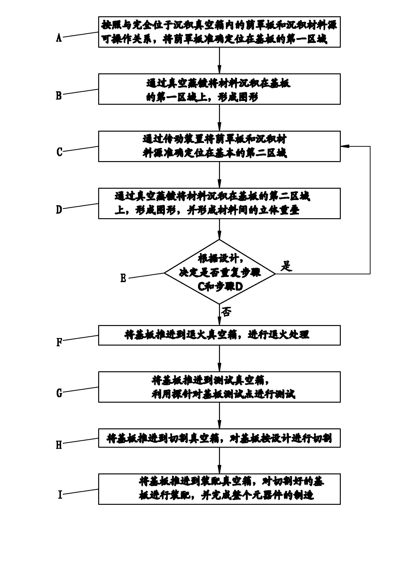
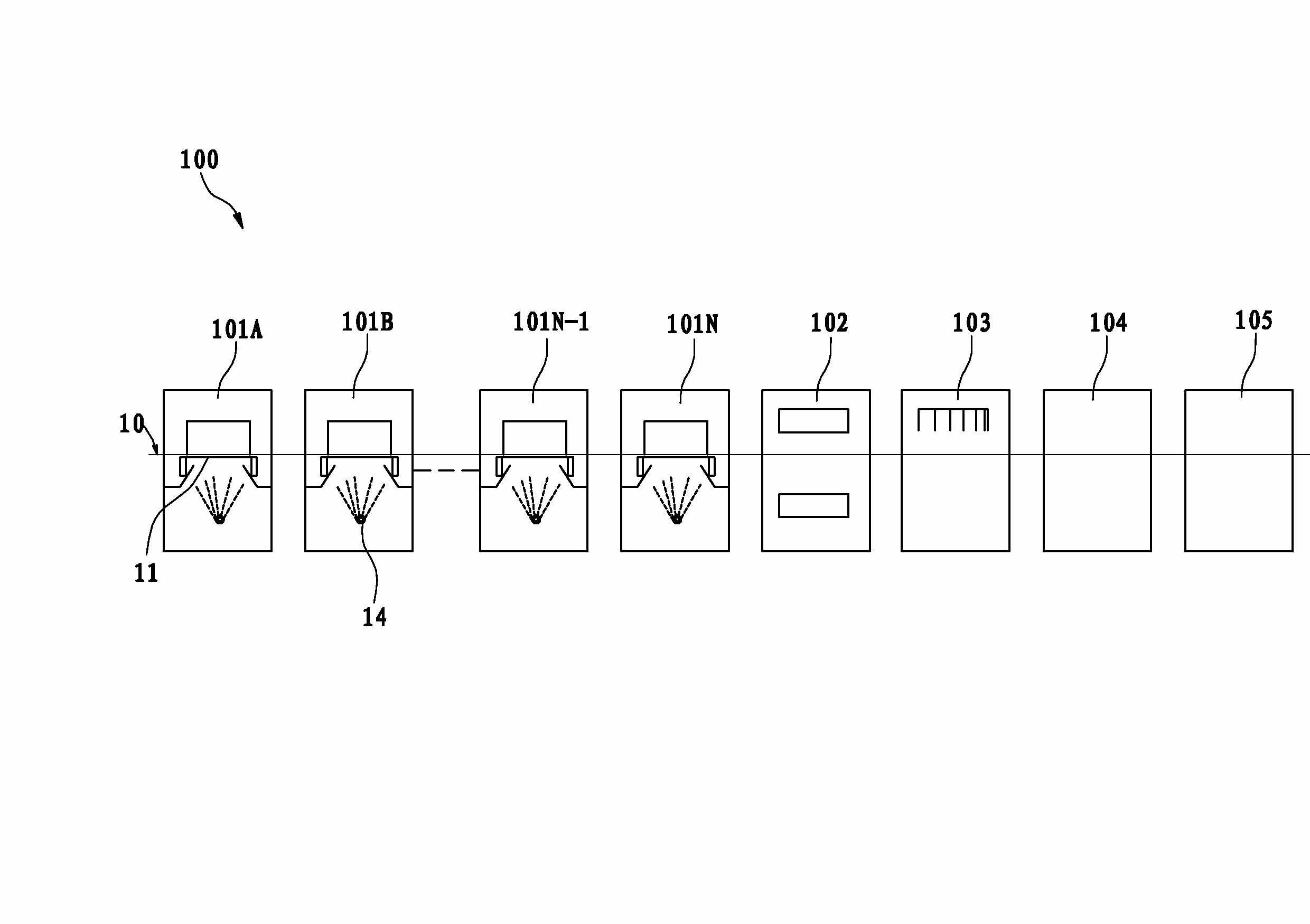
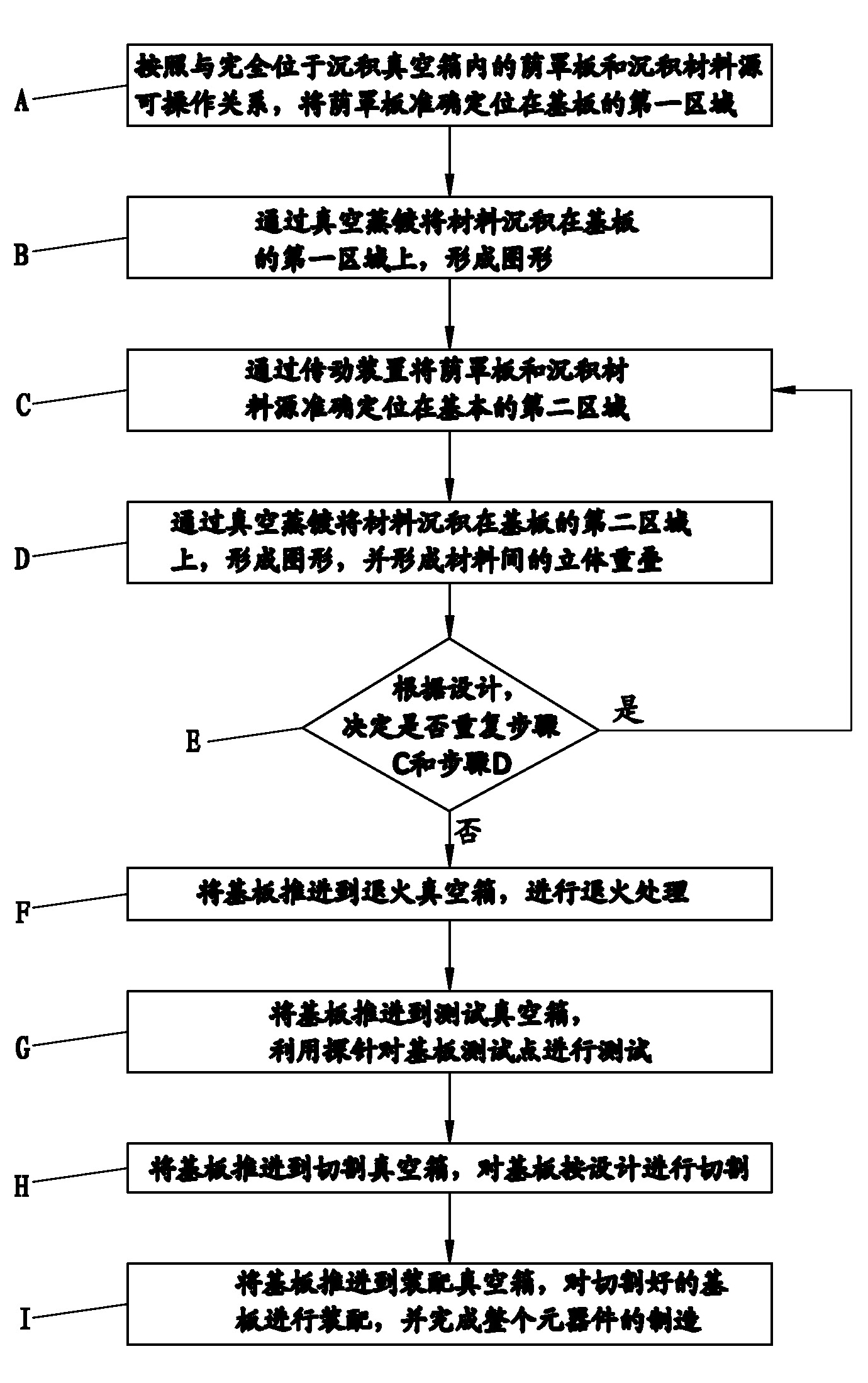
[0037] like figure 1 As shown, what it shows is a method for manufacturing devices using a shadow mask technology production line of the present invention, which includes the following steps:
[0038] A. accurately positioning the shadow mask on the first region of the substrate in operable relationship to the shadow mask and the source of deposition material positioned entirely within the deposition chamber;
[0039] B. Depositing the material on the first region of the substrate by vacuum evaporation to form a pattern;
[0040] C. Accurately position the shadow mask and the deposition material source in the basic second area through the transmission device; specifically, it can choose the way of moving the substrate or the way of moving the shadow mask to realize the positioning of the second area; When the substrate moving method is selected, the deposition vacuum box includes multiple sets arranged continuously, and the transmission device pushes the substrate to move along the deposition vacuum box so that the shadow mask and the deposition area on the substrate are accurately positioned; when the shadow mask moving method is selected , the deposition vacuum box only needs to be set to one, and the transmission device pushes the shadow mask and the deposition material source to move in the deposition vacuum box to accurately position the shadow mask and the deposition area on the substrate;
[0041] D. Deposit the material on the second area of ​​the substrate by vacuum evaporation to form a pattern and form a three-dimensional overlap between the materials; the stitching effect of the substrate can be realized by overlapping;
[0042] E. According to the design, repeat steps C and D to complete the composition and connection of components; by dividing the substrate into multiple regions, the effect of forming a large-area bottom plate from a small-area shadow mask can be realized, as one of them For the implementation method, you can refer to the expression in the Chinese patent announcement CN101027424B, which will not be elaborated here; of course, the way to realize the small-area shadow mask to form a large-area bottom plate is not limited to the above-mentioned patent announcement, for example: it can choose the method of dividing the deposition area , that is, the first area and the second area are divided into a plurality of small blocks, and by setting a set of shadow masks in each deposition vacuum box, and each set of shadow masks includes a plurality of shadow masks, and a Each of the shadow masks in the set of shadow masks corresponds to a small area in different areas, so that forming the entire substrate is achieved through separate deposition of different deposition vacuum boxes to achieve superimposition and deposition of the entire substrate; wherein, preferably , each shadow mask plate also includes a step of thoroughly cleaning the shadow mask plate after the evaporation is completed;
[0043] F. Push the substrate into the annealing vacuum box for annealing treatment; specifically, by controlling the temperature, it eliminates the stress generated in the deposition event, stabilizes the size, reduces the tendency of deformation and cracks; and plays a role in refining grains, adjusting Efficacy of organization and elimination of tissue defects;

PUM

no PUM

Description & Claims & Application Information

We can also present the details of the Description, Claims and Application information to help users get a comprehensive understanding of the technical details of the patent, such as background art, summary of invention, brief description of drawings, description of embodiments, and other original content. On the other hand, users can also determine the specific scope of protection of the technology through the list of claims; as well as understand the changes in the life cycle of the technology with the presentation of the patent timeline. Login to view more.
Why Eureka
Try Eureka