

Flat line type ion trap mass analyzer based on MEMS (micro electro mechanical system) process and manufacturing method thereof
A technology of a mass analyzer and a manufacturing method, which is applied in the field of ion trap mass spectrometers, can solve the problems of low processing accuracy, limited processing and assembly accuracy, and difficulty in batch production, so as to facilitate batch processing, reduce assembly errors, Effect of reducing ion loss
- Summary
- Abstract
- Description
- Claims
- Application Information
AI Technical Summary
Problems solved by technology
Method used
Image

Examples
Embodiment Construction
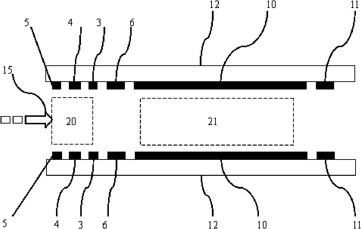
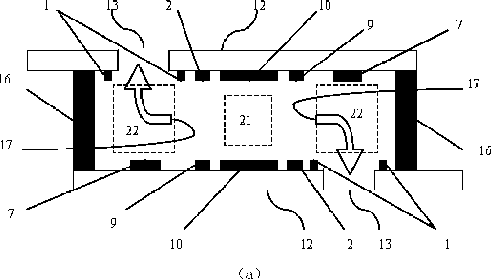
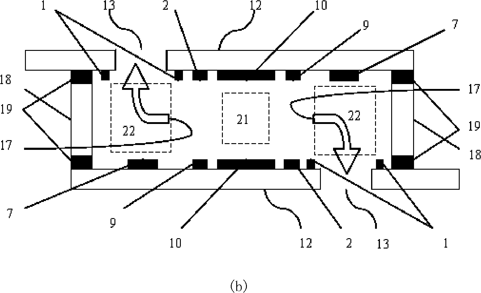
[0030] see figure 1 , 2 , a flat linear ion trap mass analyzer based on MEMS technology, including upper and lower substrates 12, and support beams supporting the upper and lower substrates 12, on the substrate 12, three pairs of upper and lower corresponding pairs are sputtered in sequence The ion lens focusing electrodes 5, 4, 3, the front gate electrode 6, the main radio frequency electrode 10, the auxiliary radio frequency electrodes 2, 9, the rear gate electrode 11, the ion exit repulsion electrodes 1, 7, pre-marked on the upper and lower substrates 12 The position is provided with a through hole as the ion outlet 13, the bonding area 8, 14 of the support beam and the borosilicate glass substrate; The silicon wafer 18 and borosilicate glass 19 of conventional thickness are cut according to a predetermined size and then electrostatically bonded twice; the area between the corresponding upper and lower ion lens focusing electrodes 5, 4, and 3 of the upper and lower substra...
PUM
 Abstract
Description
Claims
Application Information