Resistance memory device with luminescence characteristics, and operating method and application thereof

A resistive memory and resistive storage technology, which is applied in the direction of electric solid-state devices, electrical components, semiconductor devices, etc., can solve the problem of no storage and light-emitting devices, only involving light-emitting devices, etc., to improve the system self-test speed, The effect of saving cost and reducing volume

Active Publication Date: 2013-07-10
INST OF PHYSICS - CHINESE ACAD OF SCI
View PDF4 Cites 0 Cited by
  • Summary
  • Abstract
  • Description
  • Claims
  • Application Information

AI Technical Summary

Problems solved by technology

[0004] However, in modern semiconductor technology, there are many devices that use light-emitting devices for lighting and display; but in many documents and patents, either only involve pure memory cell devices, or only involve light-emitting devices, and do not combine storage and Luminescent organic bonded devices

Method used


Image

  • Resistance memory device with luminescence characteristics, and operating method and application thereof
  • Resistance memory device with luminescence characteristics, and operating method and application thereof
  • Resistance memory device with luminescence characteristics, and operating method and application thereof

Examples


Embodiment Construction

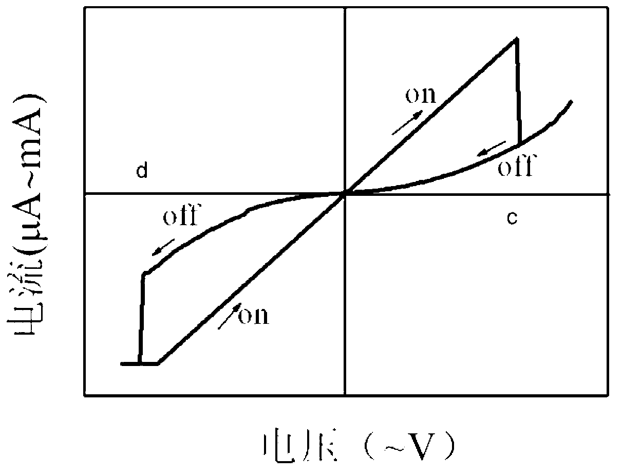
[0060] Resistive memories and their methods of operation are well known in the art and resistive memories already exist in many types of materials. The transition in which the resistance transition process is independent of the polarity of the voltage / current signal is called unipolar switching; the transition in which the resistance transition process is related to the polarity of the voltage / current signal is called bipolar switching. The transition of the system from high resistance state (off state) to low resistance state (on state) is called programming or set process, and the transition from low resistance state (on state) to high resistance state (off state) is called erasing In addition to the process (erasing or resetprocess).

[0061] like Figure 1a Shown is a schematic diagram of the resistance transition process of the unipolar transition resistance memory. For example, when the initial state is a low-resistance state, the device maintains a low resistance value...


PUM


Abstract

The invention provides a resistance memory device, which comprises a bottom electrode, a dielectric layer on the bottom electrode and a top electrode on the dielectric layer, wherein the dielectric layer is made from a material with resistance transition and luminescence characteristics; and at least one of the bottom electrode and the top electrode is transparent for light emitted from the dielectric layer. The invention also provides an operating method for the resistance memory device. The operating method comprises the following steps of: applying voltage onto the bottom electrode and thetop electrode to set the resistance state of the device to be a low resistance rate or a high impedance state; selecting a certain voltage from a voltage range which may not flip the resistance of the device, wherein the voltage can make luminous the dielectric layer; leading the light emitted from the dielectric layer out by using the transparent bottom electrode or the transparent top electrode; and identifying the resistance state of the device by utilizing the wavelength distribution of the light emitted from the dielectric layer. The invention also provides a display device and the operating method thereof.

Description

technical field [0001] The present invention relates to a resistance storage device with light emitting function, and also relates to a display device with storage function. Background technique [0002] With the rapid development of information technology, the rapid development of computer technology, the Internet and new popular electronic products, the demand for information storage products in the integrated circuit market in today's society is showing a rapid upward trend. Storage technology permeates every corner of semiconductor products. Flash memory, which occupies 90% of the market, is reported to have a limit of 32nm, and its shortcoming of low operating speed has encountered a bottleneck in development. Looking for a new generation of CMOS technology that is better than the current one Non-volatile memory devices are imperative. In recent years, resistance random access memory (Resistance Random Access Memory, referred to as RRAM) has attracted the attention and...

Claims


Application Information

Patent Timeline
Patent Type & Authority Patents(China)
IPC IPC(8): H01L45/00H01L27/24
Inventor 张培健赵宏武潘新宇孟洋刘紫玉李栋孟庆宇杨丽丽梁学锦陈东敏
Owner INST OF PHYSICS - CHINESE ACAD OF SCI
Why Eureka
Try Eureka